
5SGXMA5K1F35C1N
| Part Description |
Stratix® V GX Field Programmable Gate Array (FPGA) IC 432 46080000 490000 1152-BBGA, FCBGA |
|---|---|
| Quantity | 715 Available (as of October 7, 2026) |

| Product Category | Field Programmable Gate Array (FPGA) |
|---|---|
| Manufacturer | Intel |
| Manufacturing Status | Obsolete |
| Manufacturer Standard Lead Time | Contact Us |
| Datasheet |
Specifications & Environmental
| Device Package | 1152-FBGA (35x35) | Grade | Commercial | Operating Temperature | 0°C – 85°C | ||
|---|---|---|---|---|---|---|---|
| Package / Case | 1152-BBGA, FCBGA | Number of I/O | 432 | Voltage | 870 mV - 930 mV | ||
| Mounting Method | Surface Mount | RoHS Compliance | RoHS Compliant | REACH Compliance | REACH Unknown | ||
| Moisture Sensitivity Level | 3 (168 Hours) | Number of LABs/CLBs | 185000 | Number of Logic Elements/Cells | 490000 | ||
| Number of Gates | N/A | ECCN | 3A001A2C | HTS Code | 8542.39.0001 | ||
| Qualification | N/A | Total RAM Bits | 46080000 |
Overview of 5SGXMA5K1F35C1N – Stratix® V GX FPGA, 490,000 logic elements, ~46.08 Mbits RAM, 432 I/Os
The 5SGXMA5K1F35C1N is a Stratix V GX field-programmable gate array (FPGA) manufactured by Intel. It combines a high logic density with significant on‑chip memory and a large I/O count in a 1152‑FBGA (35×35) surface‑mount package.
Designed for complex digital designs that require substantial programmable logic, embedded memory, and extensive I/O connectivity, this commercial‑grade device is suitable for applications that need integration of many functions into a single FPGA footprint while operating within a core voltage range of 870 mV to 930 mV.
Key Features
- Core Architecture Stratix V GX family FPGA architecture provided by Intel, supporting the capability set documented in the Stratix V device datasheet.
- Logic Capacity 490,000 logic elements (logic cells) to support large-scale digital designs and dense logic implementations.
- Embedded Memory Approximately 46.08 Mbits of on‑chip RAM for buffering, packet processing, and intermediate data storage.
- I/O Density 432 user I/Os, enabling multi‑lane interfaces and broad peripheral connectivity.
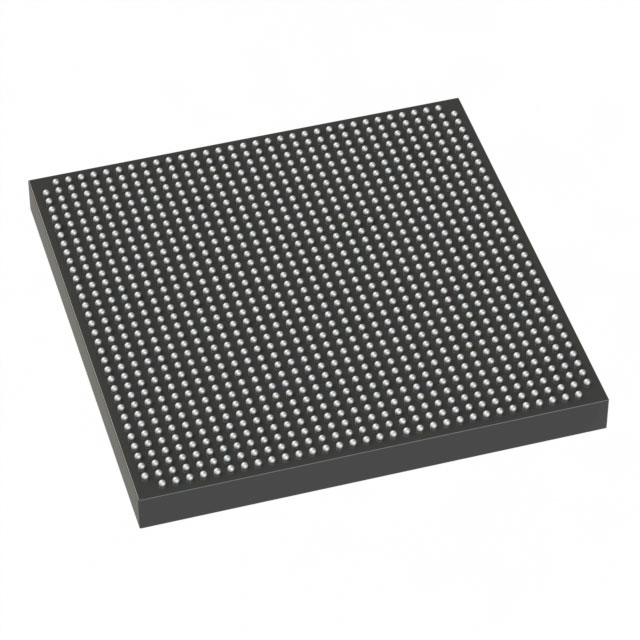
- Package 1152‑BBGA (FCBGA), supplier device package 1152‑FBGA (35×35) — compact, high‑pin‑count surface‑mount footprint.
- Power Core voltage supply range 870 mV to 930 mV for the device core.
- Temperature & Grade Commercial grade device rated for 0 °C to 85 °C operating temperature.
- Mounting Surface mount package suitable for standard PCB assembly processes.
- RoHS Compliance Device is RoHS compliant.
Typical Applications
- High‑density digital processing — Implement complex custom compute pipelines and control logic using the device's 490,000 logic elements and embedded RAM.
- Multi‑channel I/O aggregation — Consolidate numerous parallel interfaces and protocol bridges leveraging 432 user I/Os.
- Packet buffering and data staging — On‑chip memory (≈46.08 Mbits) supports buffering and intermediate data storage in networking and data acquisition systems.
- Hardware prototyping and system integration — Use the Stratix V GX device to prototype large FPGA designs and integrate multiple functions into a single package.
Unique Advantages
- High logic density: 490,000 logic elements provide headroom for complex logic and multi‑function integration, reducing the need for multiple FPGAs.
- Substantial on‑chip RAM: Approximately 46.08 Mbits of embedded memory supports packet buffering, FIFOs, and scratch storage without external RAM.
- Large I/O count: 432 I/Os enable broad peripheral and interface support directly from the FPGA.
- Compact high‑pin package: 1152‑FBGA (35×35) offers high connectivity in a compact surface‑mount footprint for space‑constrained designs.
- Low‑voltage core operation: Core supply range of 870 mV–930 mV supports modern low‑voltage FPGA power architectures.
- Commercial temperature grade: Rated 0 °C to 85 °C for standard commercial environments and applications.
Why Choose 5SGXMA5K1F35C1N?
The 5SGXMA5K1F35C1N balances high programmable logic capacity, substantial embedded memory, and a large I/O complement in a single, compact FBGA package. Its specifications make it suitable for engineers implementing complex digital systems that demand integration, on‑chip data storage, and extensive interfacing while operating within commercial temperature ranges.
This FPGA is a practical choice for teams looking to consolidate functionality onto a single device, streamline board-level design, and leverage the Stratix V GX family architecture documented in the device datasheet.
Request a quote or submit an RFQ using part number 5SGXMA5K1F35C1N to get pricing and availability information for your project planning and procurement.























Date Founded: 1968
Headquarters: Santa Clara, California, USA
Employees: 130,000+
Revenue: $54.23 Billion
Certifications and Memberships: ISO9001:2015, ISO14001:2015, ISO17025:2017, ISO27001:2022, ISO45001:2018, ISO50001:2018


