
5SGXMA5N1F45C2LN
| Part Description |
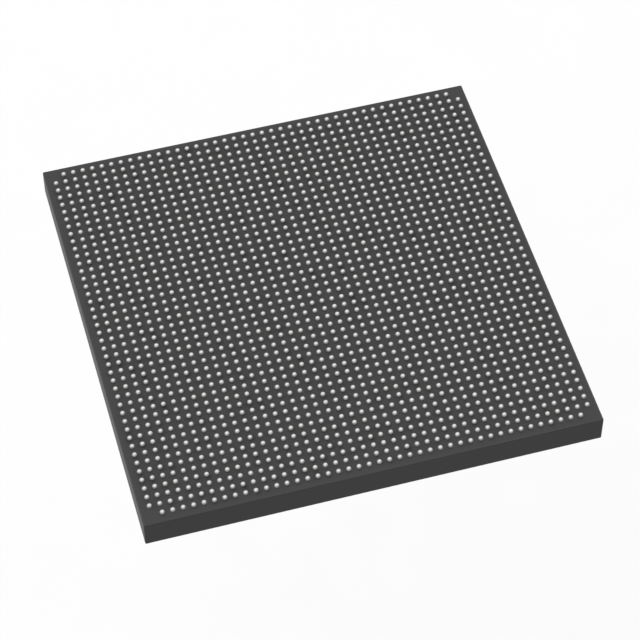
Stratix® V GX Field Programmable Gate Array (FPGA) IC 840 46080000 490000 1932-BBGA, FCBGA |
|---|---|
| Quantity | 324 Available (as of June 8, 2026) |

| Product Category | Field Programmable Gate Array (FPGA) |
|---|---|
| Manufacturer | Intel |
| Manufacturing Status | Obsolete |
| Manufacturer Standard Lead Time | Contact Us |
| Datasheet |
Specifications & Environmental
| Device Package | 1932-FBGA, FC (45x45) | Grade | Commercial | Operating Temperature | 0°C – 85°C | ||
|---|---|---|---|---|---|---|---|
| Package / Case | 1932-BBGA, FCBGA | Number of I/O | 840 | Voltage | 820 mV - 880 mV | ||
| Mounting Method | Surface Mount | RoHS Compliance | RoHS Compliant | REACH Compliance | REACH Unknown | ||
| Moisture Sensitivity Level | 3 (168 Hours) | Number of LABs/CLBs | 185000 | Number of Logic Elements/Cells | 490000 | ||
| Number of Gates | N/A | ECCN | 3A001A2C | HTS Code | 8542.39.0001 | ||
| Qualification | N/A | Total RAM Bits | 46080000 |
Overview of 5SGXMA5N1F45C2LN – Stratix® V GX Field Programmable Gate Array (FPGA), 1932-FBGA (45×45)
The 5SGXMA5N1F45C2LN is a Stratix V GX field programmable gate array (FPGA) IC designed for high-density, programmable digital designs. It combines a large logic fabric with substantial on-chip memory and a high I/O count to address complex, memory- and I/O‑intensive implementations.
With a commercial temperature rating and a low-voltage core operating range, this device is targeted at designs that require significant programmable logic capacity, abundant embedded memory, and a compact ball-grid FCBGA package for system-level integration.
Key Features
- Core Logic — Approximately 490,000 logic elements for implementing large, complex digital designs.
- Embedded Memory — Approximately 46 Mbits of on-chip RAM to support buffering, packet processing, and local data storage.
- I/O Density — 840 general-purpose I/O pins to enable high‑pin-count interfaces and parallel connectivity.
- Power — Core supply voltage range of 820 mV to 880 mV for the FPGA core power domain.
- Package and Mounting — 1932-ball BGA (FCBGA) package, supplier device package 1932‑FBGA, FC (45×45); surface-mount device for compact board-level integration.
- Temperature Grade — Commercial operating temperature range of 0 °C to 85 °C.
- Compliance — RoHS compliant for environmental compatibility.
Typical Applications
- High-density programmable logic — Implement complex state machines, control logic, and large combinational/sequential designs using the device’s extensive logic resources.
- Memory‑intensive processing — Leverage approximately 46 Mbits of embedded RAM for buffering, packet queues, and local scratchpad storage in data-path designs.
- I/O‑heavy interface aggregation — Use the 840 I/O pins to consolidate multiple high‑pin-count interfaces or parallel buses on a single FPGA.
- System integration in compact boards — The 1932‑ball FCBGA package supports high integration density where board space is constrained.
Unique Advantages
- High logic capacity: Approximately 490,000 logic elements allow large designs to be implemented without partitioning across multiple devices.
- Substantial on‑chip RAM: Approximately 46 Mbits of embedded memory reduces reliance on external RAM and simplifies board-level memory architectures.
- Very high I/O count: 840 I/O pins support extensive peripheral connectivity and multi-channel interfaces.
- Compact system-level package: 1932‑ball FCBGA (45×45) provides a dense package option for space-constrained PCBs.
- Energy-aware core supply: Low core voltage range (820–880 mV) aligns with modern power-optimized FPGA core domains.
- Regulatory readiness: RoHS compliance supports environmentally conscious product development.
Why Choose 5SGXMA5N1F45C2LN?
The 5SGXMA5N1F45C2LN positions itself as a high-capacity Stratix V GX FPGA for designers who need large logic and embedded memory in a compact, high‑pin-count package. Its combination of approximately 490,000 logic elements, roughly 46 Mbits of on‑chip RAM, and 840 I/Os makes it suitable for complex, memory- and I/O-dense FPGA implementations that require a commercial-temperature device.
Backed by Stratix V family documentation and manufacturer datasheet guidance, this device is appropriate for development teams seeking scalable programmable logic, significant on‑chip resources, and a package optimized for board-level integration.
Request a quote or submit an inquiry to obtain pricing, lead times, and availability for the 5SGXMA5N1F45C2LN.


Date Founded: 1968
Headquarters: Santa Clara, California, USA
Employees: 130,000+
Revenue: $54.23 Billion
Certifications and Memberships: ISO9001:2015, ISO14001:2015, ISO17025:2017, ISO27001:2022, ISO45001:2018, ISO50001:2018


