
5SGXMA5N1F45C2N
| Part Description |
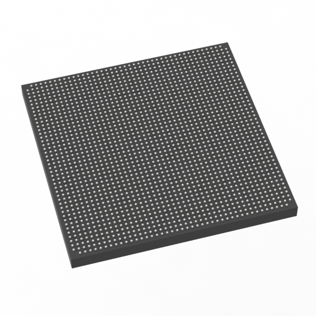
Stratix® V GX Field Programmable Gate Array (FPGA) IC 840 46080000 490000 1932-BBGA, FCBGA |
|---|---|
| Quantity | 1,729 Available (as of June 17, 2026) |

| Product Category | Field Programmable Gate Array (FPGA) |
|---|---|
| Manufacturer | Intel |
| Manufacturing Status | Obsolete |
| Manufacturer Standard Lead Time | Contact Us |
| Datasheet |
Specifications & Environmental
| Device Package | 1932-FBGA, FC (45x45) | Grade | Commercial | Operating Temperature | 0°C – 85°C | ||
|---|---|---|---|---|---|---|---|
| Package / Case | 1932-BBGA, FCBGA | Number of I/O | 840 | Voltage | 870 mV - 930 mV | ||
| Mounting Method | Surface Mount | RoHS Compliance | RoHS Compliant | REACH Compliance | REACH Unknown | ||
| Moisture Sensitivity Level | 3 (168 Hours) | Number of LABs/CLBs | 185000 | Number of Logic Elements/Cells | 490000 | ||
| Number of Gates | N/A | ECCN | 3A001A2C | HTS Code | 8542.39.0001 | ||
| Qualification | N/A | Total RAM Bits | 46080000 |
Overview of 5SGXMA5N1F45C2N – Stratix® V GX FPGA, 490,000 logic elements
The 5SGXMA5N1F45C2N is a Stratix V GX Field Programmable Gate Array (FPGA) from Intel, delivered in a 1932-BBGA FCBGA package for surface-mount assembly. This commercial-grade device provides high programmable logic density and substantial on-chip memory to support complex digital designs.
With a core supply range of 870 mV to 930 mV, up to 840 I/Os, and series-level transceiver capability documented for Stratix V GX devices, the part is suited to applications that need large-scale logic, abundant I/O, and significant embedded RAM within a compact FCBGA footprint.
Key Features
- Logic Density Approximately 490,000 logic elements, enabling implementation of large, complex logic designs and system integration on a single device.
- Embedded Memory Approximately 46 Mbits of on-chip RAM, providing substantial block RAM resources for buffering, on-chip data storage, and state machines.
- I/O Capacity Up to 840 user I/Os to support wide parallel interfaces, multiple high-pin-count peripherals, and complex board-level connectivity.
- Transceiver Capability (Series Information) Stratix V GX series documentation specifies GX transceiver speed grades up to 14.1 Gbps, reflecting the family’s support for high-speed serial links (series-level information from the device datasheet).
- Power and Voltage Core supply voltage specified from 870 mV to 930 mV for the device core.
- Package & Mounting 1932-BBGA (FCBGA) package, supplier device package noted as 1932-FBGA, FC (45×45); surface-mount mounting type simplifies high-density PCB assembly.
- Commercial Grade Operating Range Rated for commercial temperature operation from 0 °C to 85 °C.
- Regulatory RoHS compliant.
Typical Applications
- High-speed serial communication systems Leverages the Stratix V GX family’s documented transceiver speed grades and large logic fabric to implement protocol handling and SERDES-based links.
- Network and telecom processing High logic density and abundant I/O make the device suitable for packet processing, switching logic, and interface bridging within commercial networking equipment.
- Data-path acceleration and processing Large embedded RAM and logic resources support data buffering, pipeline processing, and custom accelerator functions.
- Test, measurement, and imaging Wide I/O count and on-chip memory enable capture, preprocessing, and control tasks in instrumentation and imaging systems.
Unique Advantages
- High integration density: Combines approximately 490,000 logic elements with about 46 Mbits of embedded memory to consolidate complex systems into a single FPGA.
- Extensive I/O support: Up to 840 I/Os provide flexibility for parallel interfaces, multiple peripherals, and complex board-level routing.
- Family-level high-speed serial capability: Stratix V GX series documentation includes transceiver speed grades that support multi-gigabit links, enabling high-throughput serial communication designs.
- Compact FCBGA package: The 1932-BBGA (1932-FBGA, 45×45) package delivers high pin count in a compact surface-mount form factor for dense PCB implementations.
- Commercial temperature support: Rated 0 °C to 85 °C for deployments in commercial environments where that operating range is required.
- RoHS compliant: Meets environmental compliance requirements for lead-free assembly and regulatory conformance.
Why Choose 5SGXMA5N1F45C2N?
The 5SGXMA5N1F45C2N delivers substantial programmable logic, on-chip memory, and large I/O capacity in a high-pin-count FCBGA package, making it a strong option for commercial designs that require consolidation of complex digital functions and high-bandwidth interfaces. As a member of the Stratix V GX family, its series-level capabilities for high-speed serial transceivers further extend its applicability to communication-focused solutions.
This device is well suited to designers and system architects building commercial networking, data-path acceleration, instrumentation, and other high-density FPGA applications who need a balance of logic capacity, embedded RAM, and extensive I/O in a surface-mount package.
Request a quote or submit an inquiry to receive pricing, availability, and lead-time information for the 5SGXMA5N1F45C2N.


Date Founded: 1968
Headquarters: Santa Clara, California, USA
Employees: 130,000+
Revenue: $54.23 Billion
Certifications and Memberships: ISO9001:2015, ISO14001:2015, ISO17025:2017, ISO27001:2022, ISO45001:2018, ISO50001:2018


