
5SGXMA5N1F45C2G
| Part Description |
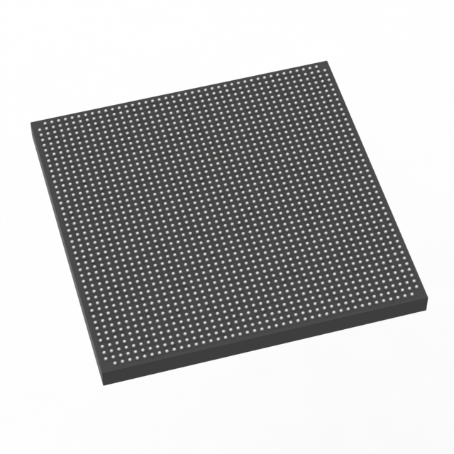
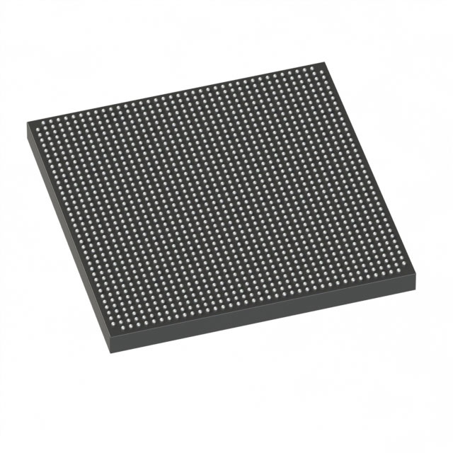
Stratix® V GX Field Programmable Gate Array (FPGA) IC 840 46080000 490000 1932-BBGA, FCBGA |
|---|---|
| Quantity | 920 Available (as of June 15, 2026) |
| Product Category | Field Programmable Gate Array (FPGA) |
|---|---|
| Manufacturer | Intel |
| Manufacturing Status | Active |
| Manufacturer Standard Lead Time | 26 Weeks |
| Datasheet |
Specifications & Environmental
| Device Package | 1932-FBGA, FC (45x45) | Grade | Commercial | Operating Temperature | 0°C – 85°C | ||
|---|---|---|---|---|---|---|---|
| Package / Case | 1932-BBGA, FCBGA | Number of I/O | 840 | Voltage | 870 mV - 930 mV | ||
| Mounting Method | Surface Mount | RoHS Compliance | RoHS Compliant | REACH Compliance | REACH Unaffected | ||
| Moisture Sensitivity Level | 3 (168 Hours) | Number of LABs/CLBs | 185000 | Number of Logic Elements/Cells | 490000 | ||
| Number of Gates | N/A | ECCN | N/A | HTS Code | N/A | ||
| Qualification | N/A | Total RAM Bits | 46080000 |
Overview of 5SGXMA5N1F45C2G – Stratix® V GX Field Programmable Gate Array (FPGA)
The 5SGXMA5N1F45C2G is a Stratix V GX family FPGA offered in a 1932‑BBGA FCBGA package. It provides a high-density programmable logic fabric with substantial embedded memory and a large number of I/O to support complex system designs.
Designed for commercial‑grade applications, this device addresses designs requiring approximately 490,000 logic elements, roughly 46.08 Mbits of on‑chip RAM, and up to 840 I/O pins. Series documentation for Stratix V GX devices details high‑speed transceiver capability (up to 14.1 Gbps per channel in applicable speed grades).
Key Features
- Core logic capacity Approximately 490,000 logic elements for implementing large, complex digital designs.
- Embedded memory Approximately 46.08 Mbits of on‑chip RAM to support buffering, FIFOs, and on‑chip data storage.
- I/O density Up to 840 I/O pins, enabling extensive external connectivity for parallel interfaces and board-level routing.
- Transceiver capability (series) Stratix V GX family documentation lists GX channel transceiver operation up to 14.1 Gbps in applicable speed grades, supporting high‑bandwidth serial links (series specification).
- Power and supply Core supply voltage range: 870 mV to 930 mV, enabling defined core power planning and regulation.
- Commercial temperature grade Rated for 0 °C to 85 °C operating temperature—suitable for commercial applications.
- Package and mounting 1932‑BBGA (FCBGA) package; supplier device package listed as 1932‑FBGA, FC (45×45), with surface‑mount mounting type.
- RoHS compliant Device complies with RoHS requirements for lead‑free assembly and environmental compliance.
Typical Applications
- High‑density digital systems Implements large, complex logic designs that require hundreds of thousands of logic elements and substantial on‑chip memory.
- High‑bandwidth serial interfaces Leverages the Stratix V GX family transceiver capabilities for designs needing multi‑Gbps serial links (per series documentation).
- Compute and acceleration Provides the logic density and memory resources commonly required for custom acceleration engines and packet processing logic.
- Prototyping and system integration Large I/O count and dense packaging support board‑level integration and mezzanine connections in prototype platforms.
Unique Advantages
- High integration density: Large logic element count and multi‑Mbit embedded memory reduce the need for external FPGA fabric partitioning and lower BOM complexity.
- Extensive I/O budget: 840 I/Os enable broad peripheral connectivity and flexible board routing for complex systems.
- Commercial thermal profile: 0 °C to 85 °C rating aligns the device with commercial application deployment and thermal planning.
- Defined core power window: Narrow core supply range (870–930 mV) simplifies regulator selection and power sequencing strategies.
- RoHS conformity: Compliant status supports lead‑free manufacturing and environmental requirements.
Why Choose 5SGXMA5N1F45C2G?
The 5SGXMA5N1F45C2G combines a very large logic fabric, substantial embedded RAM, and a high I/O count within a compact 1932‑BBGA FCBGA package, making it a fit for commercial applications that demand on‑chip capacity and connectivity. Series documentation for Stratix V GX devices also documents multi‑Gbps transceiver capability for designs that require high‑speed serial links.
This device is suited to engineers and system designers building high‑density FPGA implementations where on‑chip memory, logic scale, and I/O availability drive architecture choices. Its commercial grade, RoHS compliance, and defined electrical parameters support reliable integration into production designs.
Request a quote or submit an inquiry to obtain pricing, availability, and additional technical support for the 5SGXMA5N1F45C2G.


Date Founded: 1968
Headquarters: Santa Clara, California, USA
Employees: 130,000+
Revenue: $54.23 Billion
Certifications and Memberships: ISO9001:2015, ISO14001:2015, ISO17025:2017, ISO27001:2022, ISO45001:2018, ISO50001:2018


