
5SGXMA5N1F45C2LG
| Part Description |
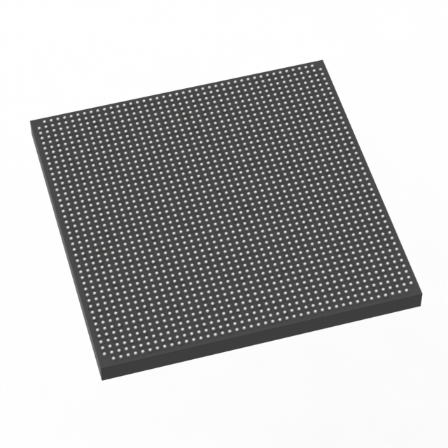
Stratix® V GX Field Programmable Gate Array (FPGA) IC 840 46080000 490000 1932-BBGA, FCBGA |
|---|---|
| Quantity | 670 Available (as of June 14, 2026) |

| Product Category | Field Programmable Gate Array (FPGA) |
|---|---|
| Manufacturer | Intel |
| Manufacturing Status | Active |
| Manufacturer Standard Lead Time | 26 Weeks |
| Datasheet |
Specifications & Environmental
| Device Package | 1932-FBGA, FC (45x45) | Grade | Commercial | Operating Temperature | 0°C – 85°C | ||
|---|---|---|---|---|---|---|---|
| Package / Case | 1932-BBGA, FCBGA | Number of I/O | 840 | Voltage | 820 mV - 880 mV | ||
| Mounting Method | Surface Mount | RoHS Compliance | RoHS Compliant | REACH Compliance | REACH Unaffected | ||
| Moisture Sensitivity Level | 3 (168 Hours) | Number of LABs/CLBs | 185000 | Number of Logic Elements/Cells | 490000 | ||
| Number of Gates | N/A | ECCN | N/A | HTS Code | N/A | ||
| Qualification | N/A | Total RAM Bits | 46080000 |
Overview of 5SGXMA5N1F45C2LG – Stratix® V GX Field Programmable Gate Array (FPGA) IC, 1932-BBGA FCBGA
The 5SGXMA5N1F45C2LG is a commercial-grade Stratix V GX FPGA in a 1932-BBGA FCBGA package. It delivers high on-chip capacity with approximately 490,000 logic elements and approximately 46 Mbits of embedded memory, making it suitable for high-density, compute- and I/O-intensive designs.
Packaged as a surface-mount 1932-FBGA (45×45) device with up to 840 I/Os and a core voltage supply range of 820 mV to 880 mV, this device targets applications that require large logic resource counts, substantial embedded RAM, and significant I/O integration within a commercial temperature range (0 °C to 85 °C).
Key Features
- Core logic — Approximately 490,000 logic elements to implement large-scale digital logic, custom accelerators, and complex control/state machines.
- Embedded memory — Approximately 46 Mbits of on-chip RAM for buffering, packet storage, and on-chip data structuring.
- I/O capacity — Up to 840 I/Os to support dense external interfacing, parallel bus implementations, and multi-channel connectivity.
- Package and mounting — 1932-BBGA, FCBGA (supplier device package: 1932-FBGA, FC, 45×45) in a surface-mount form factor for system-level integration.
- Power supply — Core voltage supply range of 820 mV to 880 mV for designs targeting Stratix V core operating conditions.
- Commercial temperature grade — Rated for 0 °C to 85 °C operation (commercial grade).
- Stratix V GX family characteristics — As a member of the Stratix V GX family, the series documentation indicates GX channel transceiver speed grades available in the family (up to 14.1 Gbps for certain GX configurations).
- Regulatory status — RoHS compliant.
Typical Applications
- High-bandwidth signal processing — Large logic and embedded memory resources enable implementation of real-time processing pipelines and multi-channel data paths.
- Networking and switching — High I/O count and substantial on-chip RAM support packet buffering, parallel interface bridging, and custom switching logic.
- Prototyping and system integration — Dense logic capacity and a large I/O envelope make the device suitable for complex prototype platforms and integration into advanced systems.
Unique Advantages
- Large on-chip capacity: Approximately 490,000 logic elements and ~46 Mbits of embedded RAM reduce the need for external logic and memory, simplifying system BOM and board routing.
- High I/O density: Up to 840 I/Os enable direct interfacing to multiple parallel buses, sensors, or external devices without extensive glue logic.
- Compact, manufacturable package: 1932-BBGA FCBGA in a 45×45 supplier package supports surface-mount assembly for volume manufacturing while conserving board area.
- Commercial-grade thermal range: Rated for 0 °C to 85 °C operation, matching typical commercial embedded and enterprise system environments.
- Series-level transceiver capability: As part of the Stratix V GX family, the series documentation shows availability of high-speed GX channel options in the family, which can inform system-level planning for designs that may leverage transceiver features.
- RoHS compliant: Conforms to RoHS requirements to support regulatory needs in many regions.
Why Choose 5SGXMA5N1F45C2LG?
The 5SGXMA5N1F45C2LG is positioned for designers who need substantial on-chip logic and memory capacity combined with a high I/O count in a dense surface-mount package. Its commercial-grade rating, defined core supply window, and package density make it suitable for demanding embedded, networking, and signal-processing platforms where integration and compact board footprint are priorities.
Choosing this Stratix V GX FPGA provides a scalable foundation within the Stratix V family, offering a clear upgrade path and access to the family’s documented electrical and transceiver characteristics for informed system design and long-term product planning.
Request a quote or submit an inquiry to receive pricing, availability, and technical ordering information for the 5SGXMA5N1F45C2LG.


Date Founded: 1968
Headquarters: Santa Clara, California, USA
Employees: 130,000+
Revenue: $54.23 Billion
Certifications and Memberships: ISO9001:2015, ISO14001:2015, ISO17025:2017, ISO27001:2022, ISO45001:2018, ISO50001:2018


