
5SGXMABN3F45C2G
| Part Description |
Stratix® V GX Field Programmable Gate Array (FPGA) IC 840 53248000 952000 1932-BBGA, FCBGA |
|---|---|
| Quantity | 516 Available (as of June 14, 2026) |
| Product Category | Field Programmable Gate Array (FPGA) |
|---|---|
| Manufacturer | Intel |
| Manufacturing Status | Active |
| Manufacturer Standard Lead Time | 26 Weeks |
| Datasheet |
Specifications & Environmental
| Device Package | 1932-FBGA, FC (45x45) | Grade | Commercial | Operating Temperature | 0°C – 85°C | ||
|---|---|---|---|---|---|---|---|
| Package / Case | 1932-BBGA, FCBGA | Number of I/O | 840 | Voltage | 870 mV - 930 mV | ||
| Mounting Method | Surface Mount | RoHS Compliance | RoHS Compliant | REACH Compliance | REACH Unaffected | ||
| Moisture Sensitivity Level | 3 (168 Hours) | Number of LABs/CLBs | 359200 | Number of Logic Elements/Cells | 952000 | ||
| Number of Gates | N/A | ECCN | N/A | HTS Code | N/A | ||
| Qualification | N/A | Total RAM Bits | 53248000 |
Overview of 5SGXMABN3F45C2G – Stratix® V GX Field Programmable Gate Array (FPGA) IC, 952,000 logic elements, ~53.2 Mbits RAM, 840 I/Os
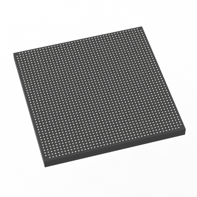
The 5SGXMABN3F45C2G is a Stratix® V GX family FPGA in a 1932-ball FCBGA package designed for commercial-temperature applications. It integrates high logic density, substantial on-chip memory, and a large I/O count to address complex digital designs requiring significant programmable logic and connectivity.
Key device characteristics provided for this part include 952,000 logic elements, approximately 53.2 Mbits of embedded memory, 840 user I/Os, a low-voltage core supply range (870 mV to 930 mV), and a commercial operating temperature range of 0 °C to 85 °C. The device is RoHS compliant and supplied in a surface-mount 1932-FBGA package (45 × 45 mm).
Key Features
- Core / Logic Contains 952,000 logic elements to implement large-scale, complex digital functions and custom architectures.
- Embedded Memory Approximately 53.2 Mbits of on-chip RAM for buffering, packet processing, and state storage without external memory in many use cases.
- I/O Capacity 840 user I/Os provide extensive external connectivity for parallel interfaces, multi-lane links, and board-level system integration.
- Package 1932-ball FCBGA (supplier package: 1932-FBGA, FC (45×45)) in a surface-mount form factor to support high pin counts and dense board layouts.
- Power Core supply range specified at 870 mV to 930 mV for low-voltage core operation.
- Temperature & Grade Commercial grade with an operating temperature range of 0 °C to 85 °C.
- Compliance RoHS compliant.
Typical Applications
- Telecommunications & Networking High logic density and extensive I/O count make this device suitable for packet processing, protocol bridging, and interface aggregation functions.
- High‑Performance Computing Acceleration Large logic resource and substantial on-chip RAM support custom accelerators and data-path engines for compute-intensive tasks.
- Prototyping and System Validation Dense programmable logic and rich I/O allow system architects to implement and validate complex digital subsystems on silicon.
- Instrumentation & Test High I/O count and embedded memory enable capture/processing pipelines and real-time data buffering for measurement systems.
Unique Advantages
- High logic density: 952,000 logic elements provide ample resources to integrate multiple subsystems into a single device, reducing board-level complexity.
- Significant on‑chip memory: Approximately 53.2 Mbits of embedded RAM reduces dependency on external memory for many buffering and state-storage tasks.
- Extensive external connectivity: 840 I/Os enable flexible interfacing to a wide range of peripherals, multi-lane links, and parallel buses.
- Compact, production-ready package: 1932-ball FCBGA surface-mount packaging supports high-pin-count designs in a standardized 45 × 45 mm footprint.
- Commercial operating range: Rated for 0 °C to 85 °C operation for mainstream commercial deployments.
- RoHS compliant: Meets common environmental compliance requirements for board-level assembly.
Why Choose 5SGXMABN3F45C2G?
This Stratix V GX FPGA part offers a combination of high programmable logic capacity, substantial embedded memory, and a large I/O complement packaged in a 1932-ball FCBGA suitable for demanding commercial designs. It is positioned for engineers and teams who need to implement complex digital systems with dense integration and flexible interface requirements while operating in standard commercial environments.
For designs that require scalable programmable logic resources, on-chip memory to reduce external BOM, and broad I/O flexibility, the 5SGXMABN3F45C2G provides a feature set aligned to those priorities, backed by Stratix V family documentation and device electrical characteristics.
If you would like pricing, availability, or a formal quote for part number 5SGXMABN3F45C2G, please submit a request referencing the part number and your required quantity and delivery timeframe.


Date Founded: 1968
Headquarters: Santa Clara, California, USA
Employees: 130,000+
Revenue: $54.23 Billion
Certifications and Memberships: ISO9001:2015, ISO14001:2015, ISO17025:2017, ISO27001:2022, ISO45001:2018, ISO50001:2018


