
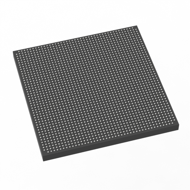
5SGXMABN3F45C4G
| Part Description |
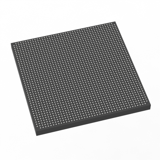
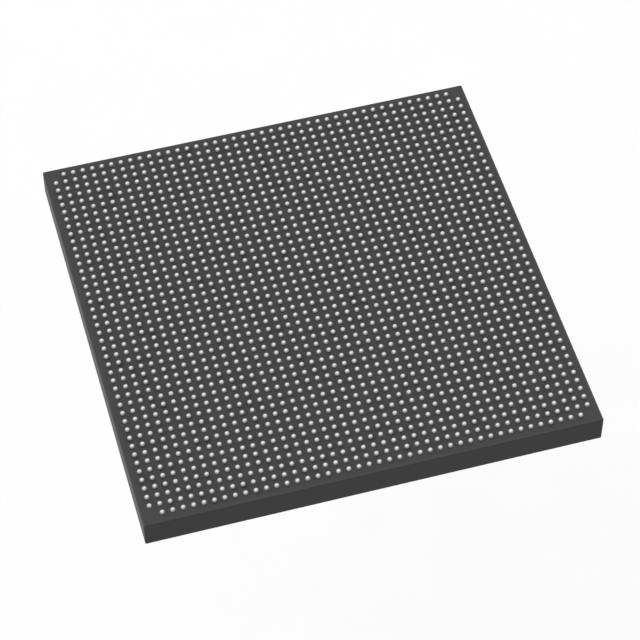
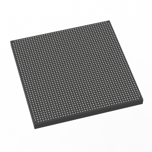
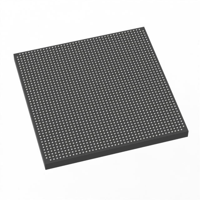
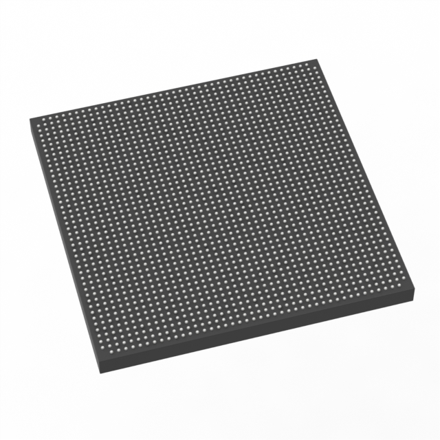
Stratix® V GX Field Programmable Gate Array (FPGA) IC 840 53248000 952000 1932-BBGA, FCBGA |
|---|---|
| Quantity | 95 Available (as of October 8, 2026) |
| Product Category | Field Programmable Gate Array (FPGA) |
|---|---|
| Manufacturer | Intel |
| Manufacturing Status | Active |
| Manufacturer Standard Lead Time | 26 Weeks |
| Datasheet |
Specifications & Environmental
| Device Package | 1932-FBGA, FC (45x45) | Grade | Commercial | Operating Temperature | 0°C – 85°C | ||
|---|---|---|---|---|---|---|---|
| Package / Case | 1932-BBGA, FCBGA | Number of I/O | 840 | Voltage | 820 mV - 880 mV | ||
| Mounting Method | Surface Mount | RoHS Compliance | RoHS Compliant | REACH Compliance | REACH Unaffected | ||
| Moisture Sensitivity Level | 3 (168 Hours) | Number of LABs/CLBs | 359200 | Number of Logic Elements/Cells | 952000 | ||
| Number of Gates | N/A | ECCN | N/A | HTS Code | N/A | ||
| Qualification | N/A | Total RAM Bits | 53248000 |
Overview of 5SGXMABN3F45C4G – Stratix® V GX Field Programmable Gate Array (FPGA) IC
The 5SGXMABN3F45C4G is a Stratix® V GX family FPGA from Intel, engineered for high-density, high-performance programmable logic applications. It combines a very large logic fabric with substantial on‑chip memory and high I/O density in a 1932‑ball FCBGA package, making it suitable for commercial designs that require significant logic resources and connectivity.
Key Features
- Core Fabric Provides 952,000 logic elements and approximately 359,200 configurable logic blocks (CLBs) to implement large, complex logic designs.
- Embedded Memory Includes approximately 53.25 Mbits of on‑chip RAM for buffering, packet processing, and local data storage.
- I/O Density Offers 840 I/O pins to support wide parallel interfaces and dense system connectivity.
- Stratix V GX Family Characteristics Part of the Stratix V GX family; the family documentation lists GX channel transceiver capabilities up to 14.1 Gbps in specific speed grades (refer to the device datasheet for details by speed grade).
- Power Core voltage supply range of 820 mV to 880 mV to match low‑voltage system architectures.
- Package & Mounting 1932‑BBGA FCBGA package (supplier device package: 1932‑FBGA, FC 45×45) and surface‑mount mounting for compact, high‑pin‑count board designs.
- Temperature & Grade Commercial grade device rated for an operating temperature range of 0 °C to 85 °C.
- Environmental Compliance RoHS compliant.
Typical Applications
- Data Center Acceleration Large logic capacity and on‑chip memory enable hardware acceleration tasks and custom compute offload in commercial data center systems.
- Networking & Telecom Infrastructure High I/O count and family transceiver capabilities (see datasheet for supported speed grades) suit packet processing, switching, and interface bridging functions.
- High‑Throughput Signal Processing Substantial logic and embedded RAM support complex DSP pipelines, FIR filters, and real‑time processing engines.
- Imaging & Video Processing Dense logic and memory resources allow implementation of multi‑channel video pipelines and image processing algorithms in commercial equipment.
Unique Advantages
- High Logic Capacity: 952,000 logic elements enable implementation of large, multi‑function systems on a single device, reducing board‑level complexity.
- Large Embedded Memory: Approximately 53.25 Mbits of on‑chip RAM minimizes external memory dependence and improves data locality for performance‑sensitive tasks.
- Extensive I/O: 840 I/O pins allow wide parallel interfaces and flexibility in system partitioning and I/O assignment.
- Compact High‑Pin Package: The 1932‑ball FCBGA (45×45) package delivers high interconnect density in a space‑efficient footprint for compact system designs.
- Low‑Voltage Core Operation: Operates between 0.82 V and 0.88 V, enabling integration with modern low‑voltage power architectures.
- Commercial‑Grade Reliability: Rated for 0 °C to 85 °C and RoHS compliant for commercial deployments.
Why Choose 5SGXMABN3F45C4G?
The 5SGXMABN3F45C4G delivers a combination of very high logic capacity, substantial embedded memory, and broad I/O in a single commercial‑grade Stratix V GX FPGA package. This makes it well suited for engineers developing complex, high‑bandwidth systems where on‑chip resources and connectivity reduce system cost and board complexity.
Choose this device for commercial applications that require scalable logic resources, significant on‑chip RAM, and a compact high‑pin‑count package, and refer to the Stratix V GX device datasheet for detailed electrical and transceiver speed‑grade specifications.
Request a quote or submit a sales inquiry for pricing and availability of 5SGXMABN3F45C4G.





















Date Founded: 1968
Headquarters: Santa Clara, California, USA
Employees: 130,000+
Revenue: $54.23 Billion
Certifications and Memberships: ISO9001:2015, ISO14001:2015, ISO17025:2017, ISO27001:2022, ISO45001:2018, ISO50001:2018


