
5SGXMB5R2F43C3N
| Part Description |
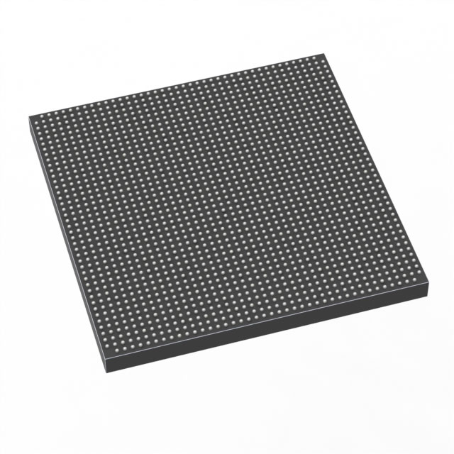
Stratix® V GX Field Programmable Gate Array (FPGA) IC 600 41984000 490000 1760-BBGA, FCBGA |
|---|---|
| Quantity | 165 Available (as of June 15, 2026) |

| Product Category | Field Programmable Gate Array (FPGA) |
|---|---|
| Manufacturer | Intel |
| Manufacturing Status | Obsolete |
| Manufacturer Standard Lead Time | Contact Us |
| Datasheet |
Specifications & Environmental
| Device Package | 1760-FCBGA (42.5x42.5) | Grade | Commercial | Operating Temperature | 0°C – 85°C | ||
|---|---|---|---|---|---|---|---|
| Package / Case | 1760-BBGA, FCBGA | Number of I/O | 600 | Voltage | 820 mV - 880 mV | ||
| Mounting Method | Surface Mount | RoHS Compliance | RoHS Compliant | REACH Compliance | REACH Unknown | ||
| Moisture Sensitivity Level | 3 (168 Hours) | Number of LABs/CLBs | 185000 | Number of Logic Elements/Cells | 490000 | ||
| Number of Gates | N/A | ECCN | 3A001A2C | HTS Code | 8542.39.0001 | ||
| Qualification | N/A | Total RAM Bits | 41984000 |
Overview of 5SGXMB5R2F43C3N – Stratix® V GX FPGA, 1760-FCBGA, 490,000 logic elements
The 5SGXMB5R2F43C3N is a Stratix® V GX Field Programmable Gate Array (FPGA) in a 1760-FCBGA package from Intel. It delivers a large programmable fabric with substantial embedded memory and a high I/O count, suited for designs that require extensive logic resources and flexible I/O timing.
As a Stratix V GX device, this part is characterized in the family datasheet for electrical and switching characteristics, including transceiver and I/O timing capabilities. The device targets applications that need significant on-chip resources, dense integration, and commercial-grade operating conditions.
Key Features
- Logic Capacity Approximately 490,000 logic elements for implementing large, complex digital designs.
- Embedded Memory Approximately 42 Mbits of total on-chip RAM to support buffering, look-up tables, and data storage within the FPGA fabric.
- I/O Density 600 user I/O pins to support wide parallel interfaces and numerous peripheral connections.
- Programmable I/O Timing Datasheet describes programmable I/O element (IOE) delay and programmable output buffer delay for fine-grained timing control.
- Transceiver Family Capability Stratix V GX family devices include GX transceiver speed grades (family-level information shows GX channel options up to 14.1 Gbps), enabling high-bandwidth serial links where required.
- Power and Supply Core voltage specified from 820 mV to 880 mV to match the device’s power requirements.
- Package & Mounting 1760-FCBGA (42.5 × 42.5 mm) package, 1760-BBGA case; surface-mount device for PCB assembly.
- Operating Conditions Commercial temperature grade with an operating range of 0 °C to 85 °C.
- Compliance RoHS compliant, meeting common environmental requirements for lead-free assembly.
Typical Applications
- High-bandwidth communications Use the Stratix V GX family transceiver capabilities and large I/O count to implement serial links and board-level interfaces that require substantial logic and I/O resources.
- Signal processing and acceleration Leverage the large logic element count and approximately 42 Mbits of embedded RAM for data-path implementations, filters, and custom hardware accelerators.
- Prototyping and complex system integration The extensive fabric and high I/O pin count support integration of multiple subsystems and rapid iteration of complex digital designs.
Unique Advantages
- Large programmable fabric: Approximately 490,000 logic elements provide headroom for complex state machines, datapaths, and control logic without partitioning across multiple devices.
- Substantial on-chip memory: Approximately 42 Mbits of embedded RAM reduces external memory dependencies and simplifies board-level design.
- High I/O count: 600 I/O pins enable broad connectivity to peripherals, wide buses, and parallel interfaces directly from the FPGA.
- Family-level transceiver options: Stratix V GX family transceiver speed grades (up to 14.1 Gbps for GX channels per the series datasheet) allow designers to plan for high-bandwidth serial link capability when needed.
- Commercial-grade thermal range: Rated for 0 °C to 85 °C operation, suitable for standard commercial electronic designs and environments.
- RoHS compliant and surface-mount package: Facilitates lead-free assembly and integration into modern PCB manufacturing flows.
Why Choose 5SGXMB5R2F43C3N?
The 5SGXMB5R2F43C3N combines a very large logic element count, generous on-chip RAM, and a high I/O count in a compact 1760-FCBGA package. It is well suited to designers who require a single-device solution for complex digital systems where integration density, embedded memory, and programmable I/O timing are priorities.
This commercial-grade Stratix V GX device also benefits from the family-level electrical and transceiver specifications documented in the series datasheet, enabling designs that anticipate high-speed serial links and precise I/O timing control while maintaining compliance with RoHS assembly requirements.
Request a quote or submit an inquiry to obtain pricing, availability, and additional technical support for integrating the 5SGXMB5R2F43C3N into your next design.


Date Founded: 1968
Headquarters: Santa Clara, California, USA
Employees: 130,000+
Revenue: $54.23 Billion
Certifications and Memberships: ISO9001:2015, ISO14001:2015, ISO17025:2017, ISO27001:2022, ISO45001:2018, ISO50001:2018


