
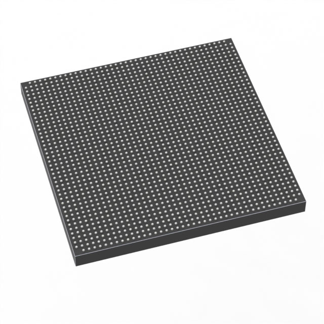
5SGXMB6R3F40C2LN
| Part Description |
Stratix® V GX Field Programmable Gate Array (FPGA) IC 432 53248000 597000 1517-FBGA (40x40) |
|---|---|
| Quantity | 16 Available (as of June 15, 2026) |

| Product Category | Field Programmable Gate Array (FPGA) |
|---|---|
| Manufacturer | Intel |
| Manufacturing Status | Obsolete |
| Manufacturer Standard Lead Time | Contact Us |
| Datasheet |
Specifications & Environmental
| Device Package | 1517-FBGA (40x40) | Grade | Commercial | Operating Temperature | 0°C – 85°C | ||
|---|---|---|---|---|---|---|---|
| Package / Case | 1517-FBGA (40x40) | Number of I/O | 432 | Voltage | 820 mV - 880 mV | ||
| Mounting Method | Surface Mount | RoHS Compliance | RoHS Compliant | REACH Compliance | REACH Unknown | ||
| Moisture Sensitivity Level | 3 (168 Hours) | Number of LABs/CLBs | 225400 | Number of Logic Elements/Cells | 597000 | ||
| Number of Gates | N/A | ECCN | 3A001A2C | HTS Code | 8542.39.0001 | ||
| Qualification | N/A | Total RAM Bits | 53248000 |
Overview of 5SGXMB6R3F40C2LN – Stratix® V GX FPGA, 1517-FBGA (40×40)
The 5SGXMB6R3F40C2LN is a Stratix® V GX field programmable gate array (FPGA) in a 1517-FBGA (40×40) package. It provides a high-density programmable fabric with 597,000 logic elements and approximately 53 Mbits of embedded RAM for complex digital designs.
Designed for commercial-grade applications, this surface-mount FPGA offers a 432-pin I/O count, low-voltage core operation, and RoHS compliance for straightforward integration into board-level systems.
Key Features
- Core Logic 597,000 logic elements to implement large-scale combinational and sequential logic functions.
- Embedded Memory Approximately 53 Mbits of on-chip RAM for data buffering, FIFOs, and memory-intensive logic.
- I/O Density 432 available I/O pins to support wide bus interfaces and multiple external peripherals.
- Power and Voltage Core supply range of 820 mV to 880 mV to match low-voltage system rails and power budgets.
- Package and Mounting 1517-FBGA (40×40) package, surface-mount for high-density PCB assembly.
- Operating Conditions Commercial temperature grade rated for 0 °C to 85 °C.
- Environmental Compliance RoHS compliant.
Unique Advantages
- High logic capacity: 597,000 logic elements enable implementation of complex RTL, integration of multiple functions, and consolidation of discrete components into a single FPGA.
- Substantial embedded memory: Approximately 53 Mbits of on-chip RAM reduce the need for external memory for many buffering and storage tasks.
- Ample I/O availability: 432 I/Os provide flexibility for interfacing with numerous high-pin-count peripherals and parallel buses.
- Low-voltage core operation: 820–880 mV supply range helps align with modern low-voltage system architectures and power-optimized designs.
- Compact BGA package: 1517-FBGA (40×40) supports high-density PCB layouts while maintaining robust mechanical and thermal characteristics for commercial applications.
- Commercial temperature rating: Specified 0 °C to 85 °C operation for standard commercial deployments.
Why Choose 5SGXMB6R3F40C2LN?
The 5SGXMB6R3F40C2LN balances high programmable logic capacity and significant embedded memory in a compact 1517-FBGA package, making it suitable for dense, board-level digital systems that require substantial on-chip resources. Its 432 I/Os and low-voltage core range support flexible integration into contemporary designs while maintaining RoHS compliance and commercial temperature operation.
This part is well suited to development teams and procurement groups looking for a high-density Stratix® V GX FPGA with verifiable on-chip resources and standard commercial-grade specifications, backed by documented Stratix V device electrical characteristics.
Request a quote or submit an inquiry to receive pricing and availability information for the 5SGXMB6R3F40C2LN.


Date Founded: 1968
Headquarters: Santa Clara, California, USA
Employees: 130,000+
Revenue: $54.23 Billion
Certifications and Memberships: ISO9001:2015, ISO14001:2015, ISO17025:2017, ISO27001:2022, ISO45001:2018, ISO50001:2018


