
5SGXMB6R3F40C3G
| Part Description |
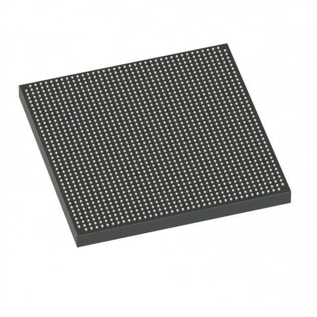
Stratix® V GX Field Programmable Gate Array (FPGA) IC 432 53248000 597000 1517-FBGA (40x40) |
|---|---|
| Quantity | 21 Available (as of June 15, 2026) |

| Product Category | Field Programmable Gate Array (FPGA) |
|---|---|
| Manufacturer | Intel |
| Manufacturing Status | Active |
| Manufacturer Standard Lead Time | 26 Weeks |
| Datasheet |
Specifications & Environmental
| Device Package | 1517-FBGA (40x40) | Grade | Commercial | Operating Temperature | 0°C – 85°C | ||
|---|---|---|---|---|---|---|---|
| Package / Case | 1517-FBGA (40x40) | Number of I/O | 432 | Voltage | 820 mV - 880 mV | ||
| Mounting Method | Surface Mount | RoHS Compliance | RoHS Compliant | REACH Compliance | REACH Unaffected | ||
| Moisture Sensitivity Level | 3 (168 Hours) | Number of LABs/CLBs | 225400 | Number of Logic Elements/Cells | 597000 | ||
| Number of Gates | N/A | ECCN | N/A | HTS Code | N/A | ||
| Qualification | N/A | Total RAM Bits | 53248000 |
Overview of 5SGXMB6R3F40C3G – Stratix® V GX Field Programmable Gate Array (FPGA) IC, 597,000 logic elements
The 5SGXMB6R3F40C3G is an Intel Stratix V GX series FPGA supplied in a 1517‑FBGA (40×40) surface‑mount package. It delivers large on‑chip logic and memory resources with 597,000 logic elements and approximately 53 Mbits of embedded RAM, plus a 432‑pin I/O count for complex system integration.
Specified for commercial operation (0 °C to 85 °C) and a core supply range of 820 mV to 880 mV, this device is targeted at high‑density, high‑integration FPGA designs that require extensive logic, memory, and I/O resources in a compact BGA footprint. The device is RoHS‑compliant.
Key Features
- Core logic density Provides 597,000 logic elements to support large-scale programmable logic implementations and complex custom architectures.
- Embedded memory Approximately 53 Mbits of on‑chip RAM to handle buffering, LUTs, and data storage without external memory in many designs.
- I/O capability 432 user I/O pins for broad connectivity to peripherals, memory, and high‑speed interfaces.
- Stratix V GX family Part of the Stratix V GX lineup, supporting the GX class transceiver architecture described in the device family datasheet for high‑speed serial applications.
- Power and core voltage Core supply range of 820 mV to 880 mV to match system power‑domain requirements and power‑delivery designs.
- Package and mounting 1517‑FBGA (40×40) surface‑mount package for compact board layouts and dense system integration.
- Commercial grade Rated for 0 °C to 85 °C operation, suitable for commercial applications and environments within this range.
- Compliance RoHS‑compliant manufacturing.
Typical Applications
- High‑density digital processing Use the 597,000 logic elements and large embedded RAM for complex signal processing, compute offload, and algorithm acceleration.
- High‑speed serial connectivity As part of the Stratix V GX family, the device supports designs that implement GX transceiver channels for multi‑Gbps serial links and protocol bridging.
- Large I/O integration With 432 I/O pins, integrate multiple peripherals, ADCs/DACs, memory interfaces, and control buses on a single FPGA device.
- Compact system designs The 1517‑FBGA (40×40) package enables dense board layouts where large logic and memory resources are required in a small form factor.
Unique Advantages
- High logic capacity: 597,000 logic elements allow implementation of complex, large‑scale programmable functions without partitioning across multiple devices.
- Substantial on‑chip RAM: Approximately 53 Mbits of embedded memory reduces dependence on external memory for buffering and intermediate storage.
- Extensive I/O: 432 user I/O pins simplify system integration by providing direct connections for many peripherals and interfaces.
- Compact BGA package: 1517‑FBGA (40×40) provides a small PCB footprint while maintaining high pin count for dense designs.
- Commercial temperature rating: Specified operation from 0 °C to 85 °C for mainstream electronic products and systems.
- RoHS compliance: Manufactured to meet RoHS requirements for lead‑free assemblies.
Why Choose 5SGXMB6R3F40C3G?
The 5SGXMB6R3F40C3G delivers a combination of large logic capacity, substantial embedded memory, and extensive I/O in a compact 1517‑FBGA package, making it suitable for complex FPGA designs that require high integration within a limited board area. Its core voltage range and commercial temperature rating provide clear electrical and environmental parameters for system design.
As a member of the Intel Stratix V GX family, this device is supported by comprehensive device documentation and electrical specifications, enabling engineering teams to plan power, timing, and I/O implementation with the documented device characteristics.
Request a quote or submit an inquiry to obtain pricing, availability, and additional technical information for the 5SGXMB6R3F40C3G.


Date Founded: 1968
Headquarters: Santa Clara, California, USA
Employees: 130,000+
Revenue: $54.23 Billion
Certifications and Memberships: ISO9001:2015, ISO14001:2015, ISO17025:2017, ISO27001:2022, ISO45001:2018, ISO50001:2018


