
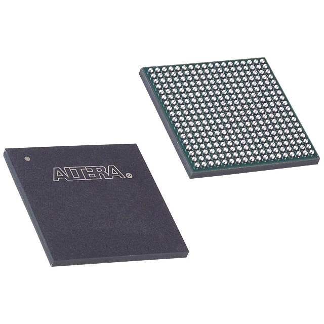
EP1C12F256C8N
| Part Description |
Cyclone® Field Programmable Gate Array (FPGA) IC 185 239616 12060 256-BGA |
|---|---|
| Quantity | 699 Available (as of June 18, 2026) |

| Product Category | Field Programmable Gate Array (FPGA) |
|---|---|
| Manufacturer | Intel |
| Manufacturing Status | Obsolete |
| Manufacturer Standard Lead Time | Contact Us |
| Datasheet |
Specifications & Environmental
| Device Package | 256-FBGA (17x17) | Grade | Commercial | Operating Temperature | 0°C – 85°C | ||
|---|---|---|---|---|---|---|---|
| Package / Case | 256-BGA | Number of I/O | 185 | Voltage | 1.425 V - 1.575 V | ||
| Mounting Method | Surface Mount | RoHS Compliance | Unknown | REACH Compliance | REACH Unknown | ||
| Moisture Sensitivity Level | 3 (168 Hours) | Number of LABs/CLBs | 1206 | Number of Logic Elements/Cells | 12060 | ||
| Number of Gates | N/A | ECCN | 3A991D | HTS Code | 8542.39.0001 | ||
| Qualification | N/A | Total RAM Bits | 239616 |
Overview of EP1C12F256C8N – Cyclone® Field Programmable Gate Array (FPGA) IC 185 239616 12060 256-BGA
The EP1C12F256C8N is a Cyclone® family FPGA offering a mid-range integration point with 12,060 logic elements and approximately 239,616 bits of embedded RAM. The Cyclone family is based on a 1.5‑V, 0.13‑µm, all-layer copper SRAM process and is positioned for cost-effective data-path and interface applications.
This device provides a balance of logic density, on-chip memory and I/O capacity—185 user I/O pins—delivered in a 256‑FBGA (17 × 17) surface-mount package. Key characteristics include dual PLLs for clocking, a defined operating voltage window, and commercial temperature grade for general embedded and system designs.
Key Features
- Logic Capacity Provides 12,060 logic elements for implementing mid-range digital designs and control logic.
- Embedded Memory Approximately 239,616 bits of on-chip RAM to support buffering, FIFOs and local data storage.
- I/O and Interface Support 185 user I/O pins enable connectivity to peripherals, memory interfaces and external logic.
- Clocking Includes two PLLs (as specified for the EP1C12 device) to support clock multiplication and phase control for multi-clock designs.
- Process and Device Family Cyclone family architecture built on a 1.5‑V, 0.13‑µm SRAM process, intended for cost-effective data-path applications.
- Package & Mounting 256‑FBGA (17 × 17) / 256‑BGA package in a surface-mount form factor for compact board integration.
- Power and Temperature Nominal supply range 1.425 V to 1.575 V; commercial operating temperature range 0 °C to 85 °C.
- Compliance RoHS compliant for regulatory alignment in common commercial applications.
Typical Applications
- High-speed data-path processing Use the device’s logic density and embedded RAM for packet processing, buffering and custom datapath functions.
- Memory interface and controllers On-chip RAM and I/O capacity support designs that interface to external DDR/SDR memory and fast-cycle memory devices.
- Peripheral and ASIC/ASSP bridging 185 I/O pins and flexible I/O standards (Cyclone family capability) enable glue-logic, protocol conversion and peripheral interfacing.
- Clocked systems and timing control Two PLLs allow clock multiplication and phase adjustments for multi-clock system requirements.
Unique Advantages
- Balanced integration: 12,060 logic elements and ~239,616 bits of embedded RAM combine to reduce external logic and simplify board-level design.
- Compact board footprint: 256‑FBGA (17 × 17) surface-mount package enables high-density mounting while preserving substantial I/O count.
- Predictable power domain: Tight supply window (1.425 V–1.575 V) provides consistent operating conditions for system power architecture.
- Commercial temperature rating: 0 °C–85 °C rating suits general embedded and consumer-facing applications.
- Clocking flexibility: Two PLLs support clock multiplication and phase shifting to meet multi-clock and timing-critical requirements.
- Family-level migration: Cyclone family support for vertical migration and design portability across device densities simplifies future scaling and re-use.
Why Choose EP1C12F256C8N?
The EP1C12F256C8N offers a practical combination of logic, memory and I/O for designers targeting mid-range FPGA-based systems. Its Cyclone family heritage delivers a cost-conscious FPGA option built on a 1.5‑V SRAM process with features aimed at data-path and interface-centric designs.
This device is well suited for teams needing a scalable, commercially graded FPGA with on-chip memory and dual PLL clocking, packaged in a compact 256‑FBGA for space-constrained boards. Family-level design flow support and migration paths further help protect development investment as requirements evolve.
Request a quote or contact sales to obtain pricing, availability and lead-time information for EP1C12F256C8N.


Date Founded: 1968
Headquarters: Santa Clara, California, USA
Employees: 130,000+
Revenue: $54.23 Billion
Certifications and Memberships: ISO9001:2015, ISO14001:2015, ISO17025:2017, ISO27001:2022, ISO45001:2018, ISO50001:2018


