
EP1C12F256I7
| Part Description |
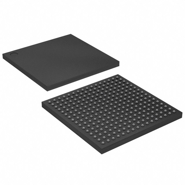
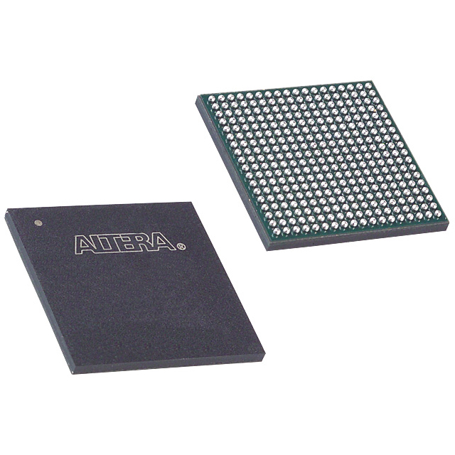
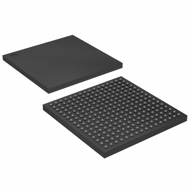
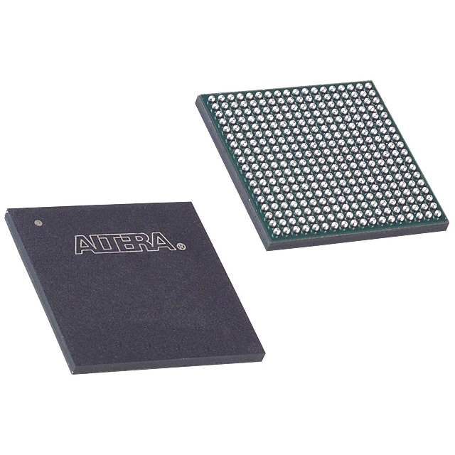
Cyclone® Field Programmable Gate Array (FPGA) IC 185 239616 12060 256-BGA |
|---|---|
| Quantity | 679 Available (as of October 7, 2026) |
| Product Category | Field Programmable Gate Array (FPGA) |
|---|---|
| Manufacturer | Intel |
| Manufacturing Status | Obsolete |
| Manufacturer Standard Lead Time | Contact Us |
| Datasheet |
Specifications & Environmental
| Device Package | 256-FBGA (17x17) | Grade | Industrial | Operating Temperature | -40°C – 100°C | ||
|---|---|---|---|---|---|---|---|
| Package / Case | 256-BGA | Number of I/O | 185 | Voltage | 1.425 V - 1.575 V | ||
| Mounting Method | Surface Mount | RoHS Compliance | RoHS non-compliant | REACH Compliance | REACH Unknown | ||
| Moisture Sensitivity Level | 3 (168 Hours) | Number of LABs/CLBs | 1206 | Number of Logic Elements/Cells | 12060 | ||
| Number of Gates | N/A | ECCN | 3A991D | HTS Code | 8542.39.0001 | ||
| Qualification | N/A | Total RAM Bits | 239616 |
Overview of EP1C12F256I7 – Cyclone® Field Programmable Gate Array (FPGA) IC 185 239616 12060 256-BGA
The EP1C12F256I7 is an Intel Cyclone® series FPGA offering 12,060 logic elements in a compact 256-ball FineLine BGA package. It is part of the Cyclone family, which is based on a 1.5‑V, 0.13‑µm, all‑layer copper SRAM process and targets cost‑sensitive data‑path and interface applications.
Designed for industrial environments, this device combines a substantial on‑chip memory resource and flexible I/O capability with on‑chip clocking resources to address control, interface, and embedded processing tasks in space‑constrained surface‑mount designs.
Key Features
- Core Logic 12,060 logic elements provide programmable combinational and sequential resources for custom logic and control functions.
- Embedded Memory Approximately 0.24 Mbits of on‑chip RAM (239,616 total RAM bits) supports buffers, FIFOs, and small on‑chip data storage.
- I/O Capacity 185 user I/O pins enable extensive external connectivity for sensors, peripherals, memories, and buses.
- Clocking Device-level support includes two PLLs for clock multiplication and phase shifting to simplify clock domain management.
- I/O Standards & Interfaces Cyclone family features include support for LVDS, SSTL, LVTTL/LVCMOS and interfaces such as DDR SDRAM and PCI standards (as implemented by the Cyclone series).
- Package & Mounting 256‑FBGA (17×17) surface‑mount package delivers a compact footprint ideal for board‑level integration.
- Supply & Power Core supply range is specified at 1.425 V to 1.575 V for reliable operation within the device’s operating window.
- Temperature Grade Industrial operating range from −40 °C to 100 °C for deployment in temperature‑challenging environments.
- Standards & Tooling Part of the Cyclone family and supported by Cyclone device documentation and development flows referenced in the Cyclone device handbook.
- RoHS Compliant Manufactured to meet RoHS environmental compliance requirements.
Typical Applications
- Data‑Path Processing Implements custom data‑path logic, buffering and protocol translation where on‑chip RAM and moderate logic density are required.
- Memory Interface Controller Acts as a bridge or controller for external memories (DDR/SDRAM), leveraging on‑chip PLLs for synchronous interfaces.
- High‑Speed I/O Gateways Supports LVDS and other high‑speed I/O standards (per Cyclone family capabilities) for interfacing between high‑speed peripherals and system logic.
- Embedded Control & Glue Logic Consolidates peripheral control, bus interfacing, and sequencing functions into a single surface‑mount FPGA to reduce component count.
Unique Advantages
- Balanced Logic and Memory: 12,060 logic elements combined with approximately 0.24 Mbits of embedded memory provide a practical balance for mid‑range embedded designs.
- Flexible I/O Density: 185 I/O pins in a 256‑FBGA package enable rich peripheral connectivity while keeping board area compact.
- Industrial Temperature Range: Rated from −40 °C to 100 °C to support deployments in industrial or temperature‑variable environments.
- Integrated Clocking: Two on‑chip PLLs simplify multi‑clock designs and timing management for memory and high‑speed interfaces.
- Compact Surface‑Mount Package: 256‑FBGA (17×17) offers a space‑efficient footprint for modern PCB layouts and product miniaturization.
- Standards‑Oriented Family Features: As a Cyclone device, it supports common I/O standards and interface modes used in data‑path and system integration tasks.
Why Choose EP1C12F256I7?
The EP1C12F256I7 positions itself as a capable mid‑density Cyclone FPGA delivering a combination of programmable logic, embedded memory, and substantial I/O in a compact 256‑FBGA package. Its industrial temperature rating and RoHS compliance make it suitable for long‑life, deployable electronic systems that require reliable on‑board programmability.
This device is well suited to engineers building mid‑range control, interface, and memory‑centric designs where a cost‑sensitive, surface‑mount FPGA with integrated clocking and family‑level interface support is required. The Cyclone family documentation and development flow support design migration and integration across device densities in the family.
Request a quote or submit an inquiry to learn more about EP1C12F256I7 availability and pricing for your next project.





















Date Founded: 1968
Headquarters: Santa Clara, California, USA
Employees: 130,000+
Revenue: $54.23 Billion
Certifications and Memberships: ISO9001:2015, ISO14001:2015, ISO17025:2017, ISO27001:2022, ISO45001:2018, ISO50001:2018


