
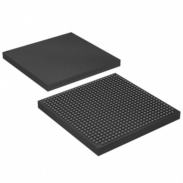
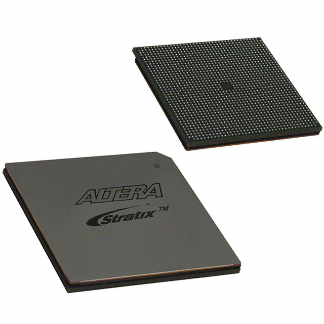
EP1SGX10CF672C7
| Part Description |
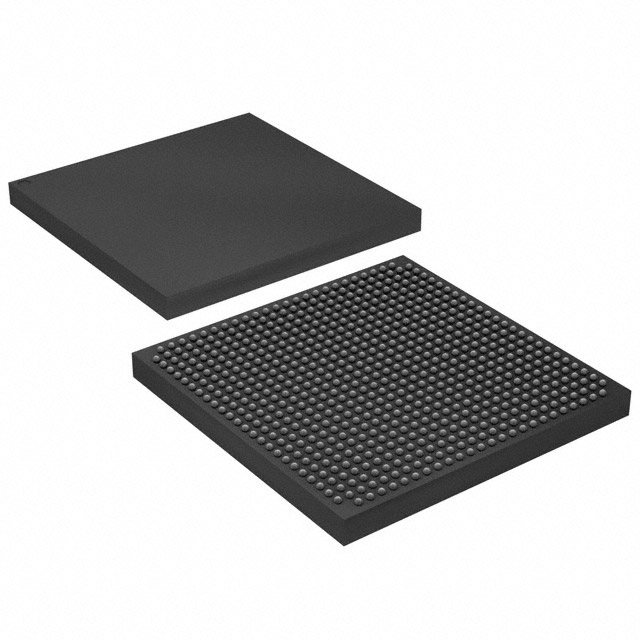
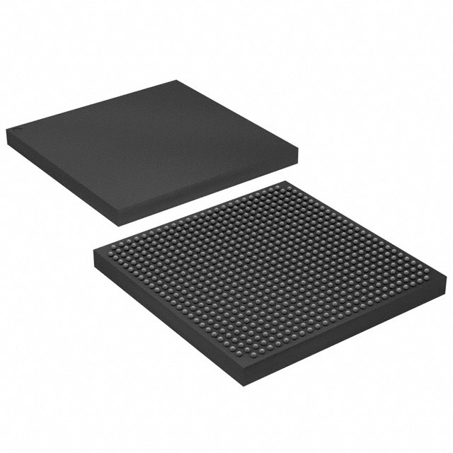
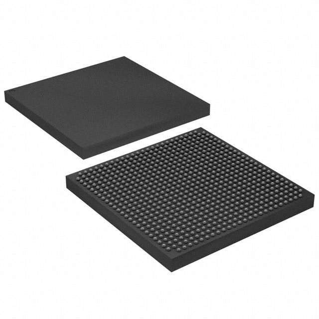
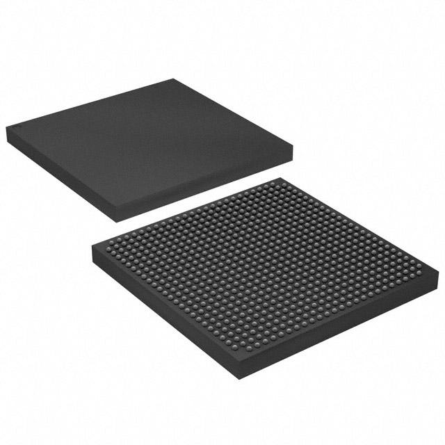
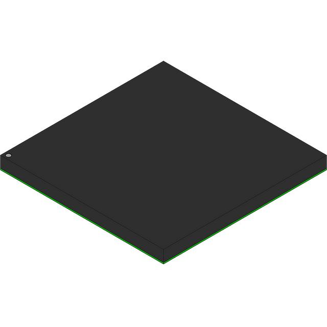
Stratix® GX Field Programmable Gate Array (FPGA) IC 362 920448 10570 672-BBGA |
|---|---|
| Quantity | 752 Available (as of October 7, 2026) |
| Product Category | Field Programmable Gate Array (FPGA) |
|---|---|
| Manufacturer | Intel |
| Manufacturing Status | Obsolete |
| Manufacturer Standard Lead Time | Contact Us |
| Datasheet |
Specifications & Environmental
| Device Package | 672-FBGA (27x27) | Grade | Commercial | Operating Temperature | 0°C – 85°C | ||
|---|---|---|---|---|---|---|---|
| Package / Case | 672-BBGA | Number of I/O | 362 | Voltage | 1.425 V - 1.575 V | ||
| Mounting Method | Surface Mount | RoHS Compliance | RoHS non-compliant | REACH Compliance | REACH Unaffected | ||
| Moisture Sensitivity Level | 3 (168 Hours) | Number of LABs/CLBs | 1057 | Number of Logic Elements/Cells | 10570 | ||
| Number of Gates | N/A | ECCN | 3A991D | HTS Code | 8542.39.0001 | ||
| Qualification | N/A | Total RAM Bits | 920448 |
Overview of EP1SGX10CF672C7 – Stratix® GX FPGA, 10,570 logic elements, 920,448‑bit RAM, 362 I/O, 672‑BGA
The EP1SGX10CF672C7 is a member of the Stratix® GX FPGA family, combining a scalable 1.5‑V logic array with high‑speed serial transceiver technology. This commercial‑grade, surface‑mount device targets high‑speed communications and system‑level interface applications such as backplane links, chip‑to‑chip interconnects, and protocol bridging.
With 10,570 logic elements, approximately 0.92 Mbits of embedded memory, and up to 362 general I/O, the device delivers a balanced mix of logic, on‑chip RAM, and I/O for applications that require high serial bandwidth and flexible I/O configurations.
Key Features
- Core Logic — 10,570 logic elements for implementing custom digital logic and control functions.
- Embedded Memory — Approximately 0.92 Mbits of on‑chip RAM organized in TriMatrix™ blocks to support true dual‑port memory and FIFO implementations.
- High‑Speed Transceivers — Family support for serial transceivers with clock data recovery (CDR) enabling full‑duplex operation from 500 Mbps to 3.1875 Gbps; programmable pre‑emphasis, equalization and VOD settings help with signal integrity tuning.
- I/O Density and Standards — 362 available I/O pins; family support for multiple single‑ended and differential I/O standards including LVDS and LVPECL on reference clocks and receiver inputs.
- DSP and Timing Resources — High‑speed DSP blocks for multiply and MAC implementations and up to 16 global clock networks with regional clocking resources per device region.
- Programmable Clocking — Up to eight general‑purpose PLLs (including enhanced and fast PLLs) for spread spectrum, bandwidth control, clock switchover, and real‑time reconfiguration.
- Reliability and Test — Built‑in self test (BIST), pattern detector/word aligner, 8B/10B encoder/decoder and channel bonding features for serial link integrity and diagnostics.
- Package and Mounting — 672‑FBGA supplier package (27 × 27 mm) in a 672‑BBGA case; surface mount for compact board integration.
- Power and Operating Range — Core supply range 1.425 V to 1.575 V; commercial operating temperature 0 °C to 85 °C. RoHS compliant.
Typical Applications
- High‑Speed Backplane Interfaces — Use the device’s serial transceivers and programmable I/O to implement multi‑lane backplane protocols and maintain signal integrity across high‑speed links.
- Chip‑to‑Chip Connectivity — Implement point‑to‑point and multi‑channel chip interconnects that require deterministic logic and embedded memory for buffering and alignment.
- Protocol Bridging and Aggregation — Translate and aggregate data streams between different serial or parallel protocols using on‑chip logic, DSP blocks, and transceiver features such as 8B/10B encoding and rate matching.
- Communications Equipment — Support for GigE, XAUI and other serial standards at the family level makes the device suitable for networking line cards and interface modules.
Unique Advantages
- Balanced Logic and Memory — 10,570 logic elements paired with approximately 0.92 Mbits of embedded RAM provide the resources needed for medium‑complexity designs without external memory dependency.
- Integrated High‑Speed SERDES — Family transceiver capability up to 3.1875 Gbps enables high‑bandwidth serial links while offering programmable signal‑conditioning features for channel tuning.
- Flexible I/O and Standards Support — Large I/O count and support for differential signaling allow designers to implement a wide range of interface standards and board topologies.
- On‑Chip DSP and Clocking — Dedicated DSP blocks and multiple PLLs reduce the need for external acceleration or complex clocking chips, simplifying system design.
- Test and Diagnostics — Built‑in self test, pattern detectors, and alignment features help validate serial links and accelerate bring‑up and debug.
- Compact, Surface‑Mount Package — 672‑FBGA (27 × 27 mm) package supports high I/O density in space‑constrained designs.
Why Choose EP1SGX10CF672C7?
The EP1SGX10CF672C7 delivers a practical combination of logic capacity, embedded memory, and high‑speed serial capability in a compact 672‑BGA surface‑mount package. As a Stratix® GX family device, it brings family‑level features such as CDR‑enabled transceivers, configurable DSP resources, and advanced clocking to designs that require deterministic performance and multi‑protocol interfacing.
This device is well suited to engineers building communications modules, interface bridging solutions, and medium‑complexity FPGA implementations where a balance of on‑chip RAM, DSP blocks, and programmable I/O can reduce external components and accelerate time to market.
Request a quote or submit your requirements to our sales team to get pricing and availability for the EP1SGX10CF672C7.





















Date Founded: 1968
Headquarters: Santa Clara, California, USA
Employees: 130,000+
Revenue: $54.23 Billion
Certifications and Memberships: ISO9001:2015, ISO14001:2015, ISO17025:2017, ISO27001:2022, ISO45001:2018, ISO50001:2018


