
EP1SGX10DF672C6
| Part Description |
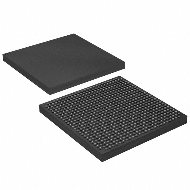
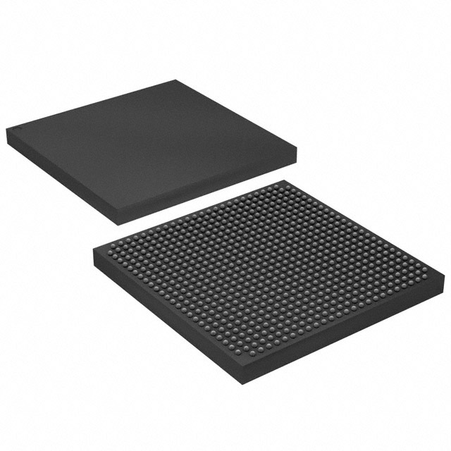
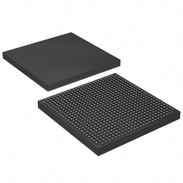
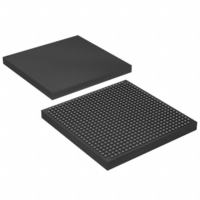
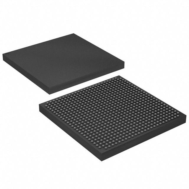
Stratix® GX Field Programmable Gate Array (FPGA) IC 362 920448 10570 672-BBGA |
|---|---|
| Quantity | 386 Available (as of October 7, 2026) |
| Product Category | Field Programmable Gate Array (FPGA) |
|---|---|
| Manufacturer | Intel |
| Manufacturing Status | Obsolete |
| Manufacturer Standard Lead Time | Contact Us |
| Datasheet |
Specifications & Environmental
| Device Package | 672-FBGA (27x27) | Grade | Commercial | Operating Temperature | 0°C – 85°C | ||
|---|---|---|---|---|---|---|---|
| Package / Case | 672-BBGA | Number of I/O | 362 | Voltage | 1.425 V - 1.575 V | ||
| Mounting Method | Surface Mount | RoHS Compliance | RoHS non-compliant | REACH Compliance | REACH Unaffected | ||
| Moisture Sensitivity Level | 3 (168 Hours) | Number of LABs/CLBs | 1057 | Number of Logic Elements/Cells | 10570 | ||
| Number of Gates | N/A | ECCN | 3A991D | HTS Code | 8542.39.0001 | ||
| Qualification | N/A | Total RAM Bits | 920448 |
Overview of EP1SGX10DF672C6 – Stratix® GX FPGA, 10,570 logic elements, 672-BBGA
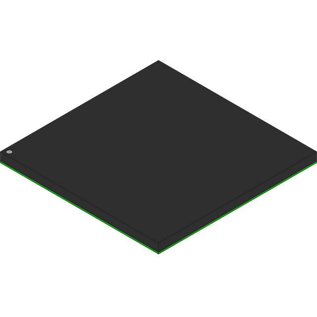
The EP1SGX10DF672C6 is a Stratix GX family field programmable gate array (FPGA) in a 672-BBGA package manufactured by Intel. This commercial-grade, surface-mount device combines a scalable high-performance logic array with the Stratix GX family’s high-speed serial transceiver technology to address demanding communications and system-integration applications.
With 10,570 logic elements, approximately 0.92 Mbits of embedded RAM, and 362 I/O pins, this device targets high-speed backplane interfaces, chip-to-chip links, and communications protocol-bridging designs where dense logic, abundant I/O, and integrated serial connectivity support system consolidation and faster time to market.
Key Features
- Logic Capacity — 10,570 logic elements (LEs) provide a substantial programmable fabric for implementing custom logic, protocol engines, and control functions.
- Embedded Memory — Approximately 0.92 Mbits of on-chip RAM to implement FIFOs, buffers, and packet/frame storage without external memory for many functions.
- I/O Count — 362 I/O pins support wide parallel interfaces and multiple high-speed I/O channels for system interconnect.
- High‑Speed Transceiver Technology (Stratix GX family) — Family-level transceivers include clock data recovery and SERDES capabilities supporting 500 Mbps to 3.1875 Gbps operation and common serial protocols for backbone and chip-to-chip links.
- TriMatrix Memory Architecture — Family architecture provides RAM blocks in multiple sizes for flexible true dual-port memory and FIFO implementations.
- Power and Supply — Core voltage supply range of 1.425 V to 1.575 V to match system power rails and design requirements.
- Package and Mount — 672-BBGA (supplier package 672-FBGA, 27×27 mm) in a surface-mount package for high-density PCB designs.
- Commercial Temperature Grade — Rated for 0 °C to 85 °C operation for standard commercial deployments.
- Standards and Integration (family) — Stratix GX family-level features include support for numerous single-ended and differential I/O standards, programmable transceiver parameters, and megafunction IP support for protocol and interface implementation.
- RoHS Compliant — Device meets RoHS environmental requirements for compliant assembly and manufacturing.
Typical Applications
- High‑speed backplane interfaces — Use the device’s dense logic, extensive I/O, and family transceiver capabilities to implement backplane protocol bridging and packet switching.
- Chip‑to‑chip serial links — Leverage the Stratix GX transceiver technology for multi‑Gbps serial channels between chips and modules.
- Communications protocol bridging — Implement protocol conversion, aggregation, and custom forwarding logic using on-chip memory and programmable fabric.
- System integration and prototyping — Combine logic, memory, and plentiful I/O for board-level integration, control functions, and hardware validation.
Unique Advantages
- Balanced logic and memory resources: 10,570 LEs and approximately 0.92 Mbits of embedded RAM support complex logic and buffering on a single device, reducing external components.
- High I/O density: 362 I/O pins accommodate wide parallel buses and multiple interfaces without extensive board-level multiplexing.
- Integrated high-speed serial capability (family): Stratix GX transceiver features enable multi‑Gbps links and protocol support, simplifying high-bandwidth interconnect design.
- Compact, surface-mount package: 672-BBGA (27×27) provides a high-pin-count solution in a compact footprint for dense PCB layouts.
- Commercial operating range and RoHS compliance: Rated 0 °C to 85 °C and RoHS compliant for standard commercial product deployments and environmentally compliant manufacturing.
- Flexible power rail support: Core supply range of 1.425 V to 1.575 V allows integration into common power architectures.
Why Choose EP1SGX10DF672C6?
The EP1SGX10DF672C6 delivers a practical combination of programmable logic, embedded memory, and abundant I/O in a compact 672-BBGA surface-mount package. As part of the Stratix GX family, it benefits from family-level high-speed serial transceiver features and a flexible memory architecture that help simplify high-bandwidth interface designs and protocol-bridging tasks.
This device is well suited for designers and system integrators building commercial networking, communications, and high-speed board-level applications that require a balanced mix of logic density, I/O capability, and on-chip memory, with the added benefit of family megafunction support for faster development cycles.
Request a quote or submit an inquiry to receive pricing and availability information for the EP1SGX10DF672C6. Our team can assist with lead times, volume pricing, and technical details to support your design planning.





















Date Founded: 1968
Headquarters: Santa Clara, California, USA
Employees: 130,000+
Revenue: $54.23 Billion
Certifications and Memberships: ISO9001:2015, ISO14001:2015, ISO17025:2017, ISO27001:2022, ISO45001:2018, ISO50001:2018


