
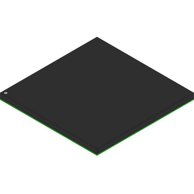
EP1SGX10DF672C5
| Part Description |
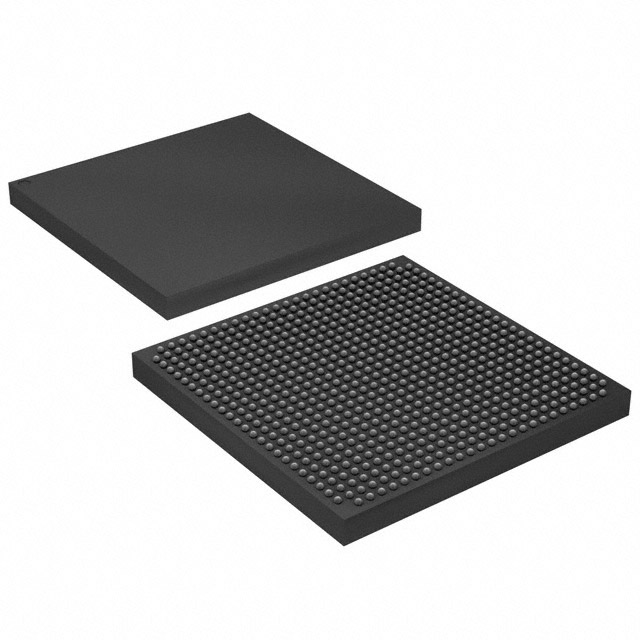
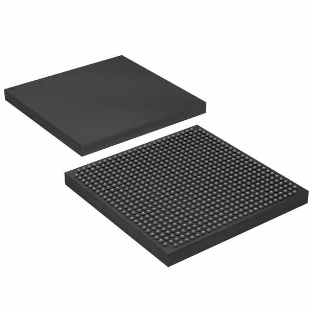
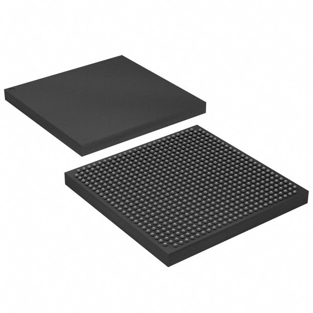
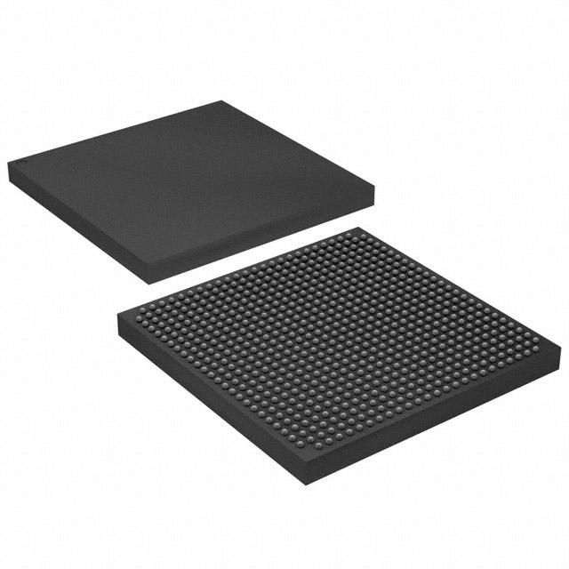
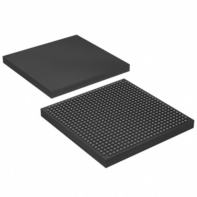
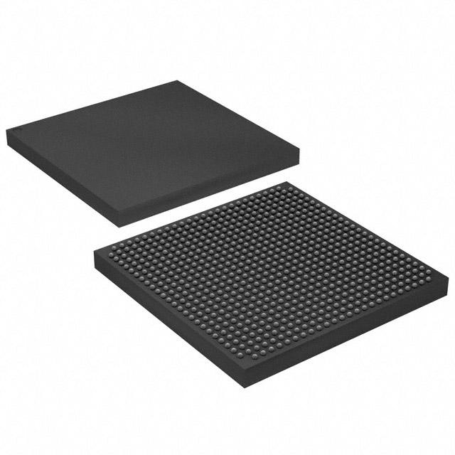
Stratix® GX Field Programmable Gate Array (FPGA) IC 362 920448 10570 672-BBGA |
|---|---|
| Quantity | 1,812 Available (as of October 8, 2026) |
| Product Category | Field Programmable Gate Array (FPGA) |
|---|---|
| Manufacturer | Intel |
| Manufacturing Status | Obsolete |
| Manufacturer Standard Lead Time | Contact Us |
| Datasheet |
Specifications & Environmental
| Device Package | 672-FBGA (27x27) | Grade | Commercial | Operating Temperature | 0°C – 85°C | ||
|---|---|---|---|---|---|---|---|
| Package / Case | 672-BBGA | Number of I/O | 362 | Voltage | 1.425 V - 1.575 V | ||
| Mounting Method | Surface Mount | RoHS Compliance | RoHS non-compliant | REACH Compliance | REACH Unaffected | ||
| Moisture Sensitivity Level | 3 (168 Hours) | Number of LABs/CLBs | 1057 | Number of Logic Elements/Cells | 10570 | ||
| Number of Gates | N/A | ECCN | 3A991D | HTS Code | 8542.39.0001 | ||
| Qualification | N/A | Total RAM Bits | 920448 |
Overview of EP1SGX10DF672C5 – Stratix® GX Field Programmable Gate Array (FPGA) IC 362 920448 10570 672-BBGA
The EP1SGX10DF672C5 is a commercial‑grade Stratix® GX FPGA offering a high‑performance, logic‑centric architecture with integrated high‑speed transceiver capabilities as documented for the Stratix GX family. It delivers 10,570 logic elements, approximately 0.92 Mbits of on‑chip RAM, and a high I/O count (362 pins) in a compact 672‑ball BGA package for system designs requiring substantial logic density and I/O bandwidth.
Typical target uses include high‑speed communications, protocol bridging, and backplane or chip‑to‑chip interfaces where a combination of programmable logic, embedded memory, and high I/O density is required. The device operates from a 1.425 V to 1.575 V core supply and is specified for commercial temperature operation (0 °C to 85 °C).
Key Features
- Core Logic 10,570 logic elements provide programmable logic resources for complex state machines, datapaths, and custom accelerators.
- Embedded Memory Approximately 0.92 Mbits of on‑chip RAM supports FIFOs, buffers, and local storage without external memory.
- I/O Density 362 I/O pins accommodate extensive external interfaces, multi‑lane buses, and high‑pin‑count connectivity.
- Transceiver‑Capable Architecture Built on the Stratix GX family architecture that includes high‑speed serial transceiver support and SERDES technology (family details documented in the Stratix GX datasheet).
- Package & Mounting 672‑ball BGA package (supplier package: 672‑FBGA, 27×27 mm) in a surface‑mount format for compact board layouts.
- Power Core supply range specified at 1.425 V to 1.575 V for predictable power budgeting and design integration.
- Temperature & Grade Commercial grade, rated for 0 °C to 85 °C operation.
- Compliance RoHS compliant for regulatory and environmental alignment.
Typical Applications
- High‑speed communications Implement protocol bridging and packet processing functions where programmable SERDES support and dense logic are required.
- Backplane and chip‑to‑chip interfaces Leverage the device’s high I/O count and Stratix GX transceiver architecture for multi‑lane backplane links and board‑to‑board communication.
- Custom protocol and interface bridging Use the FPGA’s logic elements and embedded memory for format conversion, buffering, and timing adaptation between disparate subsystems.
Unique Advantages
- Balanced logic and memory resources 10,570 logic elements paired with approximately 0.92 Mbits of embedded RAM enable mid‑range logic implementations with on‑chip storage.
- High I/O capacity 362 I/Os allow extensive peripheral and bus integration without external GPIO expanders.
- Compact, production‑ready packaging 672‑ball BGA (27×27 mm supplier package) supports high‑density PCB designs while maintaining serviceability.
- Predictable power envelope Clearly defined core supply (1.425 V–1.575 V) simplifies power supply design and thermal planning.
- Commercial temperature suitability Specified 0 °C to 85 °C operation fits a wide range of industrial and commercial electronics applications.
- Regulatory alignment RoHS compliance supports product deployment in regulated markets.
Why Choose EP1SGX10DF672C5?
The EP1SGX10DF672C5 combines a mid‑range logic element count with substantial on‑chip RAM and high I/O density in a compact BGA package, delivering a practical balance of performance, integration, and board‑level footprint for communications and interface‑centric designs. Its Stratix GX family architecture provides access to high‑speed transceiver capabilities and established FPGA toolchain support for power‑management features.
This device suits designers and procurement teams targeting scalable, production‑oriented programmable logic for commercial applications where deterministic supply requirements, package density, and I/O flexibility are key selection criteria.
Request a quote or submit a request for quotation to receive pricing and availability for EP1SGX10DF672C5 and to begin integrating this Stratix GX FPGA into your project planning.





















Date Founded: 1968
Headquarters: Santa Clara, California, USA
Employees: 130,000+
Revenue: $54.23 Billion
Certifications and Memberships: ISO9001:2015, ISO14001:2015, ISO17025:2017, ISO27001:2022, ISO45001:2018, ISO50001:2018


