
EP1SGX25CF672C5
| Part Description |
Stratix® GX Field Programmable Gate Array (FPGA) IC 455 1944576 25660 672-BBGA |
|---|---|
| Quantity | 468 Available (as of June 15, 2026) |

| Product Category | Field Programmable Gate Array (FPGA) |
|---|---|
| Manufacturer | Intel |
| Manufacturing Status | Obsolete |
| Manufacturer Standard Lead Time | Contact Us |
| Datasheet |
Specifications & Environmental
| Device Package | 672-FBGA (27x27) | Grade | Commercial | Operating Temperature | 0°C – 85°C | ||
|---|---|---|---|---|---|---|---|
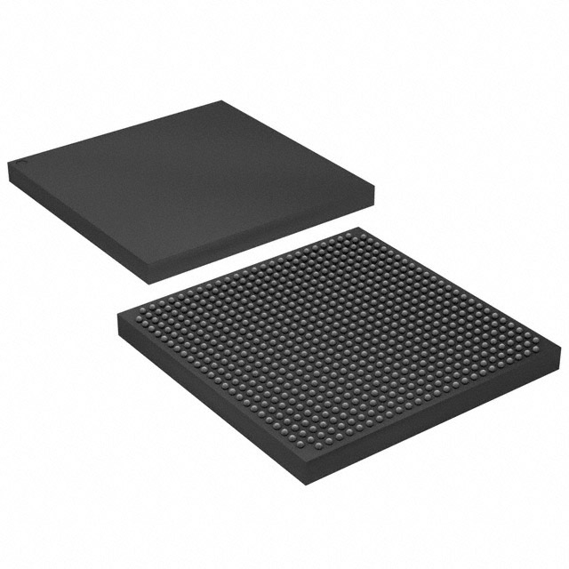
| Package / Case | 672-BBGA | Number of I/O | 455 | Voltage | 1.425 V - 1.575 V | ||
| Mounting Method | Surface Mount | RoHS Compliance | RoHS non-compliant | REACH Compliance | REACH Unknown | ||
| Moisture Sensitivity Level | 3 (168 Hours) | Number of LABs/CLBs | 2566 | Number of Logic Elements/Cells | 25660 | ||
| Number of Gates | N/A | ECCN | 3A001A7A | HTS Code | 8542.39.0001 | ||
| Qualification | N/A | Total RAM Bits | 1944576 |
Overview of EP1SGX25CF672C5 – Stratix® GX FPGA, 25,660 Logic Elements, 1.94 Mbits RAM, 455 I/Os
The EP1SGX25CF672C5 is a Stratix® GX Field Programmable Gate Array (FPGA) IC designed for applications that require scalable, high-performance programmable logic with advanced high-speed serial capabilities. Built on the Stratix GX family architecture, this commercial-grade FPGA combines a dense logic array with on-chip memory and a large I/O complement to address demanding communication and interface tasks.
Typical use cases include high-speed backplane interfaces, chip-to-chip links, and communications protocol bridging, where integration, performance, and flexible I/O are primary design drivers.
Key Features
- Logic Density 25,660 logic elements provide mid-range programmable logic capacity for complex control, signal processing, and protocol tasks.
- Embedded Memory Approximately 1.94 Mbits of on-chip RAM for buffering, FIFOs, and packet or frame storage without external memory.
- I/O Capability 455 user I/O pins support a wide range of external interfaces and high-pin-count board designs.
- High‑Speed Transceiver Technology (family) Stratix GX family transceivers include clock data recovery (CDR) and SERDES functionality supporting 500 Mbps to 3.1875 Gbps full‑duplex operation and protocol support such as XAUI and GigE as described in the Stratix GX family documentation.
- Power and Supply Core supply range specified at 1.425 V to 1.575 V to match platform power architectures.
- Package and Mounting 672‑BBGA package (supplier device package: 672‑FBGA, 27 × 27) in a surface-mount form factor for compact board layouts.
- Operating Range Commercial operating temperature range of 0 °C to 85 °C suitable for standard embedded and communications equipment.
- Standards and Compliance RoHS compliant, meeting common environmental directives for lead‑free assembly.
Typical Applications
- High‑speed backplane interfaces Use the Stratix GX family transceiver capabilities and dense logic to implement backplane bridging, packet routing, or protocol conversion functions.
- Chip‑to‑chip connectivity Leverage on-chip SERDES and abundant I/O to build reliable, high-bandwidth links between FPGA and ASIC or between FPGAs.
- Communications protocol bridging Implement protocol translation and aggregation functions using the FPGA’s logic density and embedded memory for packet buffering and alignment.
Unique Advantages
- Well‑balanced logic and memory 25,660 logic elements paired with approximately 1.94 Mbits of embedded RAM enable complex datapath and buffering implementations without immediate dependence on external memory.
- High I/O count for flexible interfacing 455 I/Os provide designers the pin budget to support wide parallel buses, multiple SerDes lanes, or mixed-signal front ends on a single device.
- Family‑level transceiver capability Stratix GX transceiver features (CDR and SERDES up to 3.1875 Gbps) allow deployment of established serial protocols where high-speed serial links are required.
- Compact thermal footprint 672‑BBGA (27 × 27) packaging offers a high-density mounting option to minimize PCB area for space-constrained systems.
- Design and manufacturing readiness Commercial temperature grading and RoHS compliance simplify integration into standard embedded and communications product lines.
Why Choose EP1SGX25CF672C5?
The EP1SGX25CF672C5 is positioned for developers who need a commercially graded FPGA with a strong balance of logic capacity, embedded memory, and I/O resources—paired with the Stratix GX family’s high-speed serial transceiver capabilities. It is well suited to mid‑complexity designs requiring multi‑lane serial links, substantial on-chip buffering, and flexible parallel interfaces.
By combining on-chip resources and family-level serial features, this device supports scalable designs for communications, interface bridging, and high-speed system interconnects while fitting into compact board layouts and standard commercial operating environments.
Request a quote or submit a request for pricing and availability to begin integrating the EP1SGX25CF672C5 into your next design.


Date Founded: 1968
Headquarters: Santa Clara, California, USA
Employees: 130,000+
Revenue: $54.23 Billion
Certifications and Memberships: ISO9001:2015, ISO14001:2015, ISO17025:2017, ISO27001:2022, ISO45001:2018, ISO50001:2018


