
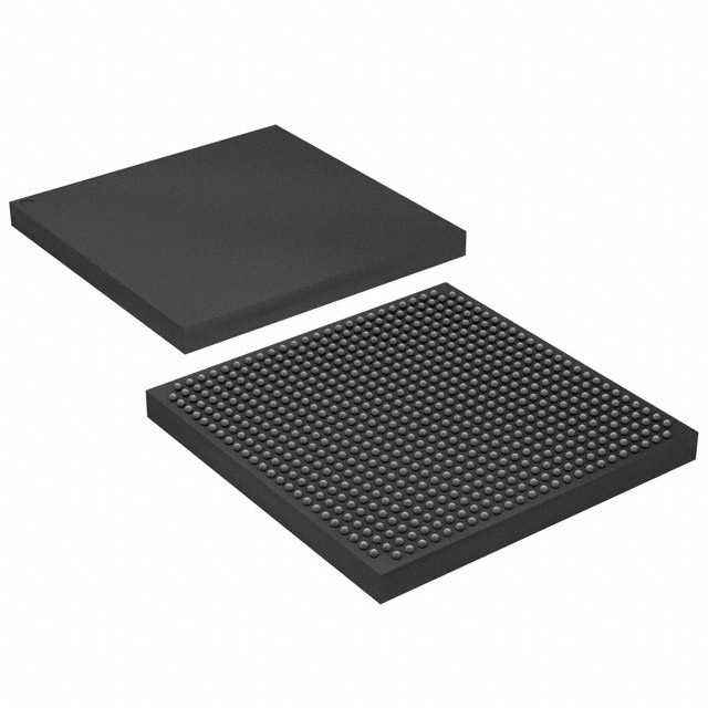
EP1SGX25CF672C6
| Part Description |
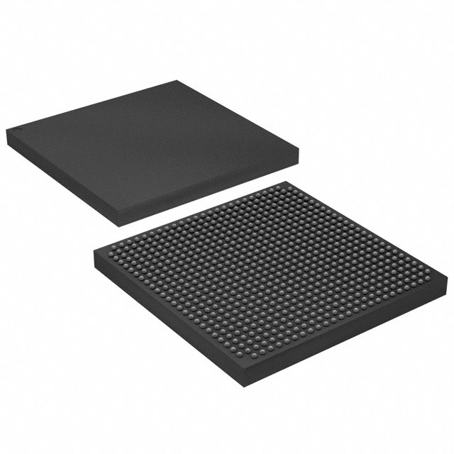
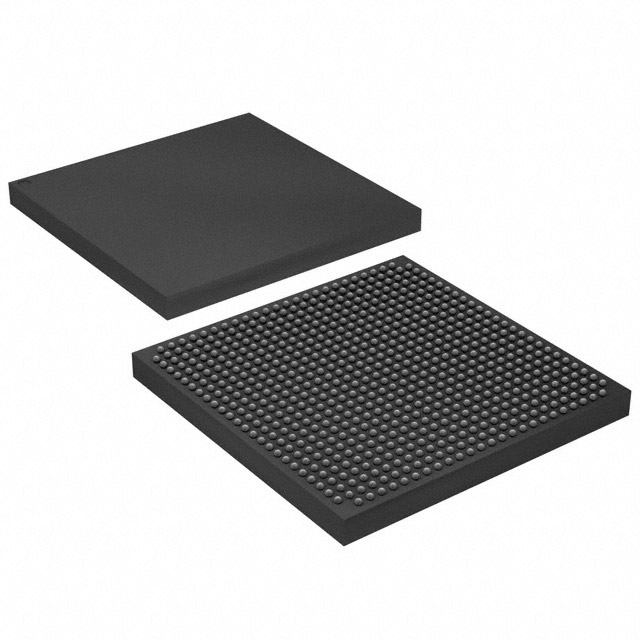
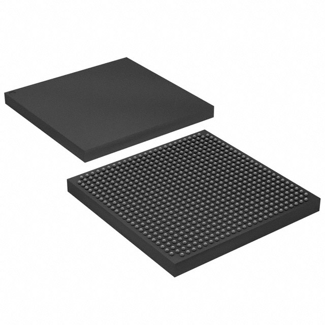
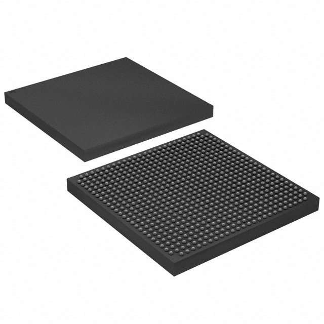
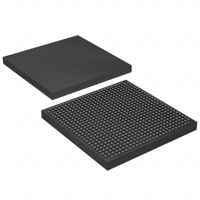
Stratix® GX Field Programmable Gate Array (FPGA) IC 455 1944576 25660 672-BBGA |
|---|---|
| Quantity | 438 Available (as of October 8, 2026) |
| Product Category | Field Programmable Gate Array (FPGA) |
|---|---|
| Manufacturer | Intel |
| Manufacturing Status | Obsolete |
| Manufacturer Standard Lead Time | Contact Us |
| Datasheet |
Specifications & Environmental
| Device Package | 672-FBGA (27x27) | Grade | Commercial | Operating Temperature | 0°C – 85°C | ||
|---|---|---|---|---|---|---|---|
| Package / Case | 672-BBGA | Number of I/O | 455 | Voltage | 1.425 V - 1.575 V | ||
| Mounting Method | Surface Mount | RoHS Compliance | RoHS non-compliant | REACH Compliance | REACH Unknown | ||
| Moisture Sensitivity Level | 3 (168 Hours) | Number of LABs/CLBs | 2566 | Number of Logic Elements/Cells | 25660 | ||
| Number of Gates | N/A | ECCN | 3A001A7A | HTS Code | 8542.39.0001 | ||
| Qualification | N/A | Total RAM Bits | 1944576 |
Overview of EP1SGX25CF672C6 – Stratix® GX Field Programmable Gate Array (FPGA) IC 455 1944576 25660 672-BBGA
The EP1SGX25CF672C6 is a Stratix® GX family FPGA from Intel designed for high-performance, high-density programmable logic applications. This device provides 25,660 logic elements, approximately 1.94 Mbits of embedded memory, and 455 I/Os in a 672-ball BGA package, delivering a balanced mix of logic capacity, on-chip RAM, and I/O bandwidth for communications and system-logic designs.
Built on the Stratix GX architecture, the family combines a 1.5‑V logic array with integrated high-speed serial transceiver technology and scalable logic resources, making it suitable for high-speed backplane interfaces, chip-to-chip links, and communications protocol bridging.
Key Features
- Logic Capacity — 25,660 logic elements to implement complex state machines, packet processing, and custom datapaths.
- Embedded Memory — Approximately 1.94 Mbits of on-chip RAM for FIFOs, buffers, and packet storage.
- I/O Resources — 455 user I/Os to support wide parallel interfaces and multiple external peripherals.
- High‑speed Transceiver Family Capabilities — Stratix GX family transceivers support full‑duplex operation from 500 Mbps to 3.1875 Gbps with features such as clock data recovery (CDR), embedded SERDES, programmable pre‑emphasis and equalization, and protocol support for XAUI, GigE, SONET/SDH and others (family-level feature set).
- Clocking and DSP Support — Family-level support includes multiple PLLs and high-speed DSP blocks for multiply-accumulate and FIR filter implementations.
- Power and Supply — Nominal core supply range of 1.425 V to 1.575 V, enabling integration with standard 1.5 V power rails.
- Package & Mounting — 672-ball BGA package (supplier package: 672-FBGA, 27×27) with surface-mount mounting for compact board integration.
- Commercial Temperature Grade — Rated for 0 °C to 85 °C operation and RoHS compliant.
Typical Applications
- High‑speed Communications — Implementation of serial protocol interfaces and line cards using family transceiver capabilities to handle XAUI, GigE, and SONET/SDH links.
- Backplane and Chip‑to‑Chip Interfaces — High I/O count and transceiver support enable use in backplane bridging, midplane routing, and chip-to-chip connectivity.
- Protocol Bridging and Packet Processing — Logic density and embedded RAM support packet buffering, protocol conversion, and real‑time processing tasks.
- Signal Processing and DSP Acceleration — On-chip memory and DSP resources support FIR filters, multiply-accumulate functions, and other signal-processing workloads.
Unique Advantages
- High Logic Density: 25,660 logic elements provide room for complex logic and system integration on a single device, reducing overall BOM and board complexity.
- Substantial On‑Chip Memory: Approximately 1.94 Mbits of embedded RAM supports deep buffering and local data storage for low-latency processing.
- Extensive I/O Count: 455 I/Os allow simultaneous connections to multiple external devices, memories, and high-speed interfaces.
- Integrated High‑Speed Serial Capabilities (Family‑Level): Stratix GX transceiver features include CDR, SERDES, and programmable equalization to simplify high-speed link implementation.
- Compact BGA Package: 672-ball BGA (672-FBGA, 27×27) surface-mount package enables dense board designs while supporting thermal and routing needs.
- Commercial‑Grade Qualification: 0 °C to 85 °C operating range and RoHS compliance for mainstream electronics applications.
Why Choose EP1SGX25CF672C6?
The EP1SGX25CF672C6 pairs sizable logic resources with substantial embedded memory and a large I/O footprint in a compact 672-ball BGA, delivering a versatile platform for high-speed communications, protocol bridging, and DSP-accelerated designs. Its core supply range and commercial temperature rating make it suitable for a wide range of mainstream system designs where performance, integration, and proven family-level transceiver features are required.
This device is well-suited for engineering teams building network interface cards, backplane controllers, and custom hardware accelerators that need a balance of logic density, on-chip RAM, and interface flexibility while relying on Intel’s Stratix GX FPGA architecture and ecosystem.
Request a quote or submit an inquiry to receive pricing, availability, and lead-time information for EP1SGX25CF672C6. Our team will provide the details you need to evaluate this device for your next design.





















Date Founded: 1968
Headquarters: Santa Clara, California, USA
Employees: 130,000+
Revenue: $54.23 Billion
Certifications and Memberships: ISO9001:2015, ISO14001:2015, ISO17025:2017, ISO27001:2022, ISO45001:2018, ISO50001:2018


