
EP20K160EFC484-1N
| Part Description |
APEX-20KE® Field Programmable Gate Array (FPGA) IC 316 81920 6400 484-BBGA |
|---|---|
| Quantity | 212 Available (as of June 15, 2026) |

| Product Category | Field Programmable Gate Array (FPGA) |
|---|---|
| Manufacturer | Intel |
| Manufacturing Status | Obsolete |
| Manufacturer Standard Lead Time | Contact Us |
| Datasheet |
Specifications & Environmental
| Device Package | 484-FBGA (23x23) | Grade | Commercial | Operating Temperature | 0°C – 85°C | ||
|---|---|---|---|---|---|---|---|
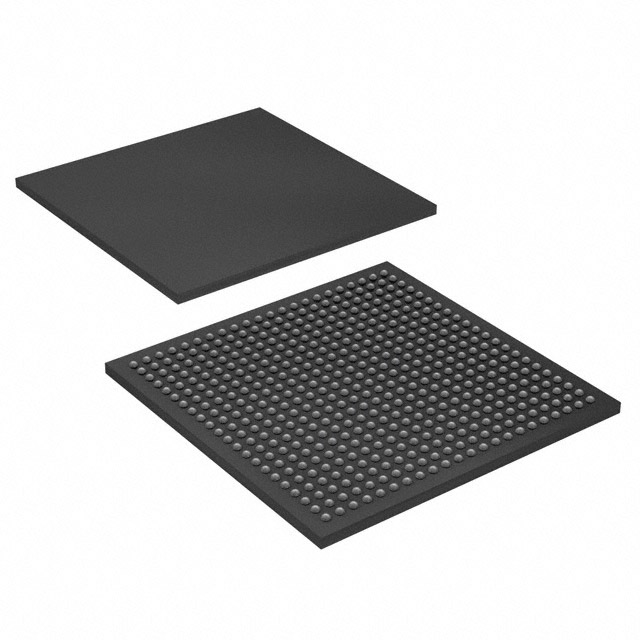
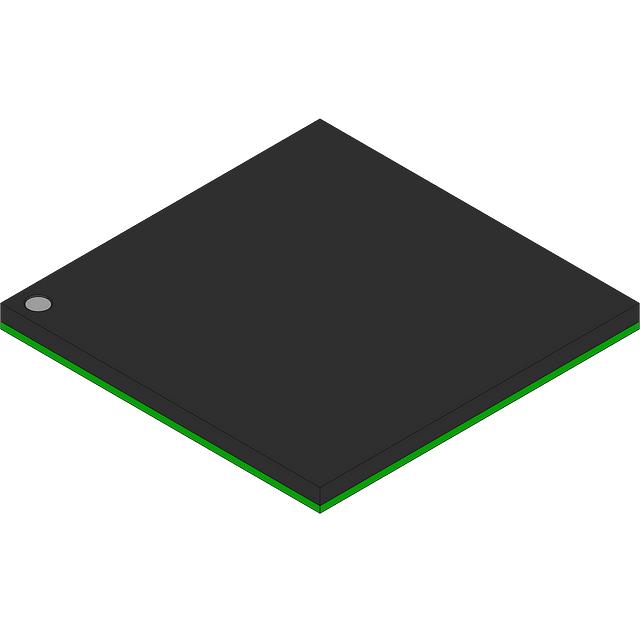
| Package / Case | 484-BBGA | Number of I/O | 316 | Voltage | 1.71 V - 1.89 V | ||
| Mounting Method | Surface Mount | RoHS Compliance | Unknown | REACH Compliance | REACH Unaffected | ||
| Moisture Sensitivity Level | 3 (168 Hours) | Number of LABs/CLBs | 640 | Number of Logic Elements/Cells | 6400 | ||
| Number of Gates | 404000 | ECCN | 3A991D | HTS Code | 8542.39.0001 | ||
| Qualification | N/A | Total RAM Bits | 81920 |
Overview of EP20K160EFC484-1N – APEX-20KE FPGA, 6,400 Logic Elements (484-BBGA)
The EP20K160EFC484-1N is an Intel APEX-20KE family field programmable gate array (FPGA) supplied in a 484-BBGA package. It combines MultiCore architecture with embedded system blocks (ESBs) to deliver configurable LUT-based logic, product-term logic and on-chip RAM for system-level integration.
Designed for commercial applications that require high-density logic, flexible I/O and on-chip memory, this device suits designs that need memory interfaces, high-speed I/O, and integrated clock management while operating within a 0 °C to 85 °C range.
Key Features
- Logic Density — 6,400 logic elements providing up to 404,000 gates for complex digital designs.
- Embedded Memory — Approximately 0.082 Mbits (81,920 bits) of on-chip RAM implemented in ESBs for FIFOs, dual-port RAM and CAM functions.
- I/O Count & Flexibility — 316 user I/O pins with MultiVolt I/O support (1.8 V, 2.5 V, 3.3 V and 5.0 V) for interoperability with a broad range of peripherals and interface voltages.
- Package & Mounting — 484-BBGA package (supplier package listed as 484-FBGA, 23×23) with surface-mount mounting.
- Supply & Temperature — Internal supply specified at 1.71 V to 1.89 V and commercial operating temperature range of 0 °C to 85 °C.
- System Integration (MultiCore Architecture) — MultiCore architecture integrates LUT logic, product-term logic and embedded memory to implement register-intensive and memory-intensive functions on-chip.
- Low-Power Design — Designed for low-power operation with support for programmable ESB power-saving modes and 1.8 V internal supply options for energy-sensitive designs.
- Clock Management — Up to four phase-locked loops (PLLs), built-in low-skew clock tree, and features such as ClockLock, ClockBoost and ClockShift for precise clock control.
- High-Speed I/O Capabilities — Bidirectional I/O performance (tCO + tSU) up to 250 MHz and LVDS support up to 840 Mbits per channel; supports advanced I/O standards including LVPECL, PCI-X, AGP, CTT, SSTL-3, SSTL-2, GTL+ and HSTL Class I.
- Memory & Bus Support — Device-level support for high-speed external memories including DDR SDRAM and ZBT SRAM, and compliance notes for PCI Local Bus operation at 3.3 V (PCI Rev. 2.2) for 33/66 MHz operation.
- Interconnect & Arithmetic — Four-level hierarchical FastTrack interconnect and dedicated carry chains for predictable routing delays and efficient arithmetic implementations.
- RoHS Compliant — Manufactured in compliance with RoHS requirements.
Typical Applications
- High-speed memory interfaces — Implement DDR SDRAM and ZBT SRAM controllers and buffers using on-chip ESBs and flexible I/O standards.
- Data acquisition and transport — Use LVDS and high-speed bidirectional I/O for multi-channel data capture, serialization and high-throughput links.
- Embedded system integration — Leverage MultiCore architecture and ESBs for on-chip FIFOs, dual-port RAM and CAM to consolidate system functions and reduce external components.
- Peripheral bridging and bus logic — Implement PCI-compliant interfaces and glue logic for system expansion, bus translation and custom peripheral control.
Unique Advantages
- Integrated memory and logic: ESBs combined with 6,400 logic elements allow implementation of both control logic and embedded buffering without large external memory dependencies.
- Flexible I/O interoperability: MultiVolt I/O support and a wide range of supported standards simplify interfacing to legacy and modern peripherals.
- Deterministic clocking: Multiple PLLs and clock features such as ClockLock and ClockShift help achieve stable, low-skew clocking for synchronous systems.
- High-density routing: FastTrack interconnect and dedicated carry chains reduce routing delay and simplify arithmetic and datapath designs.
- Commercial-grade thermal profile: Rated for 0 °C to 85 °C operation, making it appropriate for standard commercial applications and environments.
Why Choose EP20K160EFC484-1N?
The EP20K160EFC484-1N positions itself as a mid-density FPGA with a balanced mix of logic, embedded memory and versatile I/O. Its MultiCore architecture and ESB resources make it well suited for designs that require on-chip memory structures (FIFOs, dual-port RAM, CAM) alongside LUT-based logic, while the clocking and I/O features support complex timing and interface requirements.
This device is a pragmatic choice for commercial designs where integrated memory, flexible interface support and deterministic clock management reduce board-level complexity and component count, helping accelerate development and deployment.
Request a quote or submit an inquiry to receive pricing, lead-time and availability information for EP20K160EFC484-1N.


Date Founded: 1968
Headquarters: Santa Clara, California, USA
Employees: 130,000+
Revenue: $54.23 Billion
Certifications and Memberships: ISO9001:2015, ISO14001:2015, ISO17025:2017, ISO27001:2022, ISO45001:2018, ISO50001:2018


