
EP20K160EFC484-1XB
| Part Description |
APEX-20KE® Field Programmable Gate Array (FPGA) IC 316 81920 6400 484-BBGA |
|---|---|
| Quantity | 1,224 Available (as of June 15, 2026) |
| Product Category | Field Programmable Gate Array (FPGA) |
|---|---|
| Manufacturer | Intel |
| Manufacturing Status | Obsolete |
| Manufacturer Standard Lead Time | Contact Us |
| Datasheet |
Specifications & Environmental
| Device Package | 484-FBGA (23x23) | Grade | Commercial | Operating Temperature | 0°C – 85°C | ||
|---|---|---|---|---|---|---|---|
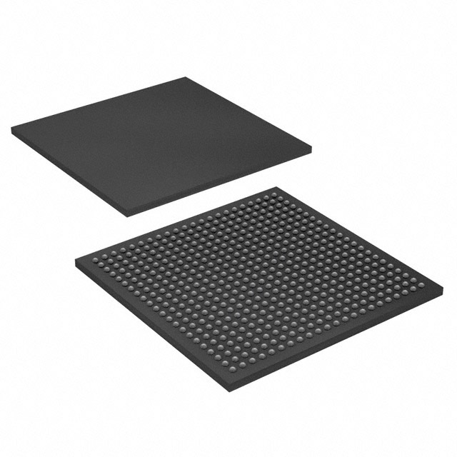
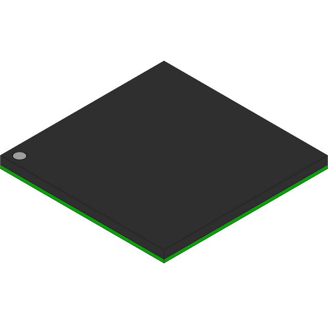
| Package / Case | 484-BBGA | Number of I/O | 316 | Voltage | 1.71 V - 1.89 V | ||
| Mounting Method | Surface Mount | RoHS Compliance | Unknown | REACH Compliance | REACH Unknown | ||
| Moisture Sensitivity Level | 3 (168 Hours) | Number of LABs/CLBs | 640 | Number of Logic Elements/Cells | 6400 | ||
| Number of Gates | 404000 | ECCN | OBSOLETE | HTS Code | 0000.00.0000 | ||
| Qualification | N/A | Total RAM Bits | 81920 |
Overview of EP20K160EFC484-1XB – APEX-20KE® Field Programmable Gate Array (FPGA) IC 316 81920 6400 484-BBGA
The EP20K160EFC484-1XB is an APEX-20KE family field programmable gate array (FPGA) from Intel. It uses the APEX 20K MultiCore architecture—combining LUT logic, product-term logic, and embedded memory—to deliver a programmable-logic building block for commercial designs that require on-chip memory, flexible I/O, and clock management.
With 6,400 logic elements, approximately 0.082 Mbits of embedded memory, and 316 I/O pins in a 484-BBGA surface-mount package, this device targets designers implementing high-density glue logic, memory interfaces, and protocol bridging within a commercial temperature range.
Key Features
- Logic Capacity — 6,400 logic elements and approximately 404,000 system gates provide ample programmable logic resources for medium-density designs.
- Embedded Memory — Approximately 81,920 bits (~0.082 Mbits) of on-chip RAM, usable for FIFOs, dual-port RAM, and content-addressable memory implementations as part of the MultiCore architecture.
- I/O Density and Package — 316 user I/O pins in a 484-BBGA package; supplier device package listed as 484-FBGA (23×23). Surface-mount mounting for compact board integration.
- Power and Voltage — Internal operating supply listed at 1.71 V to 1.89 V; designed for low-power operation consistent with the APEX 20K family.
- Flexible Clock Management — On-chip clock resources include up to four phase-locked loops (PLLs), a low-skew clock tree, and support for multiple global clock signals along with ClockLock, ClockBoost, and ClockShift features.
- High-Speed I/O Options — Family-level support for LVDS (up to 840 Mbits/channel), bidirectional I/O performance up to 250 MHz, and MultiVolt I/O interface capability to connect with 1.8 V, 2.5 V, 3.3 V, and 5.0 V signaling levels.
- External Memory and Bus Support — Documented support within the APEX 20K family for DDR SDRAM, ZBT SRAM, and compliance options for PCI Local Bus operation at 3.3 V (33/66 MHz, 32/64 bits).
- Commercial Temperature Grade — Rated for 0 °C to 85 °C operation and RoHS compliant for environmental regulatory alignment.
Typical Applications
- High-speed memory interfaces — Implement DDR SDRAM and ZBT SRAM controllers or FIFOs using the device’s embedded memory and dedicated interconnect features.
- PCI and bus bridging — Use the APEX 20K family’s documented PCI support for 3.3 V bus interfacing and bridge logic at common bus frequencies.
- High-speed differential signaling — Deploy LVDS and other high-speed I/O standards for serial links and data channels leveraging the device’s I/O performance.
- Custom protocol and glue logic — Implement protocol translation, peripheral control, and timing-critical glue logic using the device’s LUTs, product-term logic, and clocking resources.
Unique Advantages
- MultiCore architecture integration — Combines LUT logic, product-term logic, and embedded system blocks to implement both register-intensive and memory-intensive functions on a single device.
- Balanced logic and memory resources — 6,400 logic elements paired with ~0.082 Mbits of embedded RAM enable compact implementation of controllers, buffers, and state machines without external devices.
- Flexible clocking and timing — Multiple PLLs, low-skew clock tree, and programmable clock features reduce design effort for complex timing and frequency management.
- Adaptable I/O support — MultiVolt I/O interface capability and high-speed signaling options simplify integration with a wide range of system voltages and peripherals.
- Commercial-grade reliability — Rated for 0 °C to 85 °C operation and RoHS compliant, suitable for mainstream commercial electronic products.
- Compact surface-mount package — 484-BBGA footprint with 316 I/Os offers high pin count in a space-efficient BGA package for dense board layouts.
Why Choose EP20K160EFC484-1XB?
The EP20K160EFC484-1XB delivers a practical mix of programmable logic, on-chip RAM, and extensive I/O in a commercial-grade FPGA package. Its APEX 20K MultiCore architecture and documented clocking and I/O features make it well suited for developers implementing memory interfaces, bus bridging, or complex protocol logic where mid-range gate density and flexible I/O are required.
Engineers seeking a compact, RoHS-compliant FPGA with dedicated clock management and multi-voltage I/O options will find this device a capable option for commercial designs that require reliable programmability and on-chip memory resources.
To request a quote or submit a procurement inquiry for EP20K160EFC484-1XB, please provide your requirements and quantity and our team will respond with availability and pricing information.


Date Founded: 1968
Headquarters: Santa Clara, California, USA
Employees: 130,000+
Revenue: $54.23 Billion
Certifications and Memberships: ISO9001:2015, ISO14001:2015, ISO17025:2017, ISO27001:2022, ISO45001:2018, ISO50001:2018


