
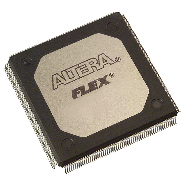
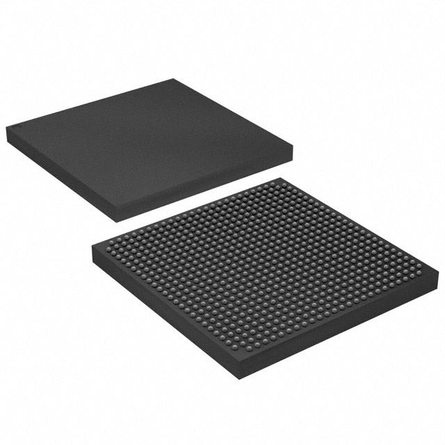
EP20K400EFC672-3N
| Part Description |
APEX-20KE® Field Programmable Gate Array (FPGA) IC 488 212992 16640 672-BBGA |
|---|---|
| Quantity | 627 Available (as of June 15, 2026) |

| Product Category | Field Programmable Gate Array (FPGA) |
|---|---|
| Manufacturer | Intel |
| Manufacturing Status | Obsolete |
| Manufacturer Standard Lead Time | Contact Us |
| Datasheet |
Specifications & Environmental
| Device Package | 672-FBGA (27x27) | Grade | Commercial | Operating Temperature | 0°C – 85°C | ||
|---|---|---|---|---|---|---|---|
| Package / Case | 672-BBGA | Number of I/O | 488 | Voltage | 1.71 V - 1.89 V | ||
| Mounting Method | Surface Mount | RoHS Compliance | Unknown | REACH Compliance | REACH Unaffected | ||
| Moisture Sensitivity Level | 3 (168 Hours) | Number of LABs/CLBs | 1664 | Number of Logic Elements/Cells | 16640 | ||
| Number of Gates | 1052000 | ECCN | 3A001A7A | HTS Code | 8542.39.0001 | ||
| Qualification | N/A | Total RAM Bits | 212992 |
Overview of EP20K400EFC672-3N – APEX-20KE® Field Programmable Gate Array, 672-BBGA
The EP20K400EFC672-3N is an APEX-20KE family field programmable gate array (FPGA) offered by Intel. It implements a MultiCore architecture that integrates look-up table (LUT) logic, product-term logic, and embedded memory, delivering a high-density, reprogrammable logic platform for complex digital designs.
Targeted at applications requiring substantial logic, memory and I/O resources, this device provides a combination of 16,640 logic elements, approximately 0.213 Mbits of embedded memory, and 488 I/O pins in a 672-BBGA package—addressing high-density system functions, memory interfacing, and multi‑domain clocking requirements.
Key Features
- High-density logic — 16,640 logic elements and 1,052,000 gates provide substantial programmable logic capacity for complex designs.
- Embedded memory — Approximately 0.213 Mbits (212,992 bits) of on-chip RAM suitable for FIFOs, dual-port RAM, and other memory functions.
- Robust I/O — 488 user I/O pins with MultiVolt I/O interface support for interfacing with multiple voltage domains.
- Flexible clock management — Family-level support for up to four PLLs and up to eight global clock signals, enabling multi-domain clocking and phase/clock-shift features.
- Advanced I/O capabilities — Family-level support includes high-speed standards and differential I/O (LVDS), and support for high-speed external memories such as DDR SDRAM and ZBT SRAM.
- Package and mounting — Surface-mount 672-BBGA package; supplier device package listed as 672-FBGA (27×27).
- Supply and temperature — Voltage supply range 1.71 V to 1.89 V and commercial operating temperature range 0 °C to 85 °C.
- Environmental — RoHS compliant.
Typical Applications
- Communications and Networking — Packet processing, protocol offload, and high-speed I/O aggregation using dense logic and extensive I/O resources.
- Memory Interface and Controllers — Implement controllers and buffering for DDR SDRAM and ZBT SRAM with on-chip RAM and high-speed I/O support.
- High‑performance Embedded Systems — Integrate custom datapaths, FIFOs and dual-port memories using embedded system blocks and abundant logic elements.
- Test & Measurement — Custom data acquisition, real-time signal routing, and protocol conversion leveraging flexible clocking and dense logic.
Unique Advantages
- Significant logic capacity: 16,640 logic elements and over one million gates enable large, integrated designs without immediate part changes.
- On-chip memory resources: Approximately 0.213 Mbits of embedded RAM reduce external memory dependence for FIFO and buffering needs.
- Wide I/O flexibility: 488 I/Os with MultiVolt interface support simplify interfacing to multiple voltage domains and legacy devices.
- Comprehensive clocking: Multiple PLLs and global clock resources support complex timing domains and phase management inside a single device.
- Commercial temperature and RoHS compliance: Commercial grade operation (0 °C to 85 °C) and RoHS compliance support common production and regulatory needs.
Why Choose EP20K400EFC672-3N?
The EP20K400EFC672-3N positions itself as a high-density, highly integrated FPGA option within the APEX-20KE family for designs that need substantial logic, embedded memory, and broad I/O capability in a single package. Its MultiCore architecture and family-level features for clock management and advanced I/O make it suitable for complex embedded systems, memory interfacing, and communications applications.
For engineering teams seeking scalability and a platform that supports memory-heavy and I/O-intensive functions, this device provides a balanced combination of programmable logic, embedded RAM, and configurable I/O in a 672-BBGA package from a recognized vendor.
Request a quote or submit your requirements to receive pricing and availability for the EP20K400EFC672-3N. Our team can help assess fit for your design and provide ordering details.


Date Founded: 1968
Headquarters: Santa Clara, California, USA
Employees: 130,000+
Revenue: $54.23 Billion
Certifications and Memberships: ISO9001:2015, ISO14001:2015, ISO17025:2017, ISO27001:2022, ISO45001:2018, ISO50001:2018


