
EP2AGX190FF35C4N
| Part Description |
Arria II GX Field Programmable Gate Array (FPGA) IC 612 10177536 181165 1152-BBGA, FCBGA |
|---|---|
| Quantity | 1,202 Available (as of June 15, 2026) |
| Product Category | Field Programmable Gate Array (FPGA) |
|---|---|
| Manufacturer | Intel |
| Manufacturing Status | Obsolete |
| Manufacturer Standard Lead Time | Contact Us |
| Datasheet |
Specifications & Environmental
| Device Package | 1152-FBGA (35x35) | Grade | Commercial | Operating Temperature | 0°C – 85°C | ||
|---|---|---|---|---|---|---|---|
| Package / Case | 1152-BBGA, FCBGA | Number of I/O | 612 | Voltage | 870 mV - 930 mV | ||
| Mounting Method | Surface Mount | RoHS Compliance | RoHS Compliant | REACH Compliance | REACH Unknown | ||
| Moisture Sensitivity Level | 3 (168 Hours) | Number of LABs/CLBs | 7612 | Number of Logic Elements/Cells | 181165 | ||
| Number of Gates | N/A | ECCN | 3A001A7A | HTS Code | 8542.39.0001 | ||
| Qualification | N/A | Total RAM Bits | 10177536 |
Overview of EP2AGX190FF35C4N – Arria II GX Field Programmable Gate Array (FPGA) IC
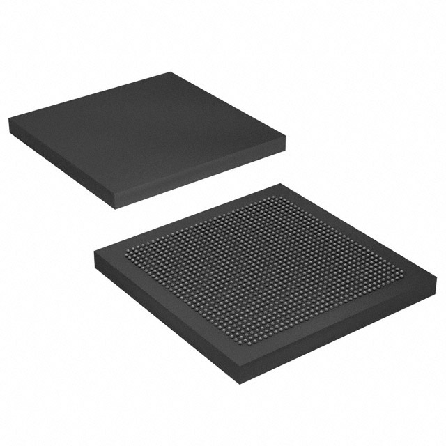
The EP2AGX190FF35C4N is an Arria II GX family FPGA from Intel, delivered in a 1152-ball FCBGA package (35 × 35). It provides a high-capacity programmable logic fabric with integrated on-chip memory and a large number of I/O for system-level integration.
Documented as part of the Arria II GX device family, the device includes transceiver and peripheral features described in the device handbook and is targeted at designs requiring substantial logic, embedded memory, and dense I/O in a surface-mount ball-grid package.
Key Features
- Logic Capacity Provides 181,165 logic elements, organized across 7,612 LABs, for complex programmable logic implementations.
- Embedded Memory Approximately 10 Mbits of on-chip RAM (10,177,536 total RAM bits) to support buffering, state machines, and data paths without external memory.
- I/O Density 612 user I/O pins to support multiple interfaces and board-level connectivity.
- Package 1152-ball BGA, FCBGA footprint (1152-FBGA, 35×35) optimized for surface-mount assembly.
- Power Supply Core voltage operating range of 870 mV to 930 mV as specified for device operation.
- Operating Temperature Rated for commercial temperature range from 0 °C to 85 °C.
- Mounting and Compliance Surface-mount device construction; RoHS compliant.
- Arria II GX Family Features (per device handbook) Electrical and switching characteristics, transceiver performance specifications and PCI Express (PIPE) HIP block details are defined in the Arria II device documentation.
Typical Applications
- High-speed serial interfaces Devices in the Arria II GX family include transceiver performance specifications suitable for designs implementing high-speed serial connectivity.
- PCI Express and system interconnect Arria II GX documentation includes PCI Express (PIPE) HIP block details, supporting implementations that require PCIe integration.
- Memory-intensive logic Designs that need substantial on-chip RAM for buffering, packet processing, or data-path staging can leverage the device’s approximately 10 Mbits of embedded memory.
- I/O-dense board interfaces With 612 I/O pins, the device supports multiple parallel interfaces and board-level connectivity without immediate reliance on external I/O expanders.
Unique Advantages
- High logic integration: The combination of 181,165 logic elements and 7,612 LABs enables complex logic consolidation into a single device, reducing PCB area and BOM count.
- Substantial on-chip RAM: Approximately 10 Mbits of embedded memory simplifies designs that require local buffering and fast on-chip storage.
- Dense I/O capability: 612 I/O pins allow flexible interface partitioning and support for multiple peripherals and high channel counts.
- Compact FCBGA package: 1152-ball FCBGA (35×35) provides a compact, surface-mount footprint suitable for space-constrained boards.
- Commercial-grade operation: Rated for 0 °C to 85 °C and RoHS compliant for standard commercial deployments.
- Documented transceiver and PCIe support: Arria II GX device handbook provides electrical, switching, and transceiver performance specifications to support high-speed interface design.
Why Choose EP2AGX190FF35C4N?
The EP2AGX190FF35C4N positions itself as a high-capacity member of the Arria II GX family, combining extensive logic resources, significant on-chip memory, and a large I/O count in a compact 1152-ball FCBGA package. It is suited for commercial designs that require integrated logic density, memory bandwidth on-chip, and documented transceiver/PCIe capabilities provided in the Arria II device handbook.
Backed by Intel’s Arria II GX documentation, this device is appropriate for engineering teams looking to consolidate complex digital functions, implement memory-intensive data paths, and integrate multiple high-speed or parallel interfaces into a single FPGA solution.
Request a quote or submit an inquiry to receive pricing and availability information for EP2AGX190FF35C4N.


Date Founded: 1968
Headquarters: Santa Clara, California, USA
Employees: 130,000+
Revenue: $54.23 Billion
Certifications and Memberships: ISO9001:2015, ISO14001:2015, ISO17025:2017, ISO27001:2022, ISO45001:2018, ISO50001:2018


