
EP2AGX190FF35C5G
| Part Description |
Arria II GX Field Programmable Gate Array (FPGA) IC 612 10177536 181165 1152-BBGA, FCBGA |
|---|---|
| Quantity | 449 Available (as of October 8, 2026) |

| Product Category | Field Programmable Gate Array (FPGA) |
|---|---|
| Manufacturer | Intel |
| Manufacturing Status | Active |
| Manufacturer Standard Lead Time | 26 Weeks |
| Datasheet |
Specifications & Environmental
| Device Package | 1152-FBGA (35x35) | Grade | Commercial | Operating Temperature | 0°C – 85°C | ||
|---|---|---|---|---|---|---|---|
| Package / Case | 1152-BBGA, FCBGA | Number of I/O | 612 | Voltage | 870 mV - 930 mV | ||
| Mounting Method | Surface Mount | RoHS Compliance | RoHS Compliant | REACH Compliance | REACH Unaffected | ||
| Moisture Sensitivity Level | 3 (168 Hours) | Number of LABs/CLBs | 7612 | Number of Logic Elements/Cells | 181165 | ||
| Number of Gates | N/A | ECCN | 3A991D | HTS Code | 8542.39.0001 | ||
| Qualification | N/A | Total RAM Bits | 10177536 |
Overview of EP2AGX190FF35C5G – Arria II GX Field Programmable Gate Array (FPGA), 1152-BBGA
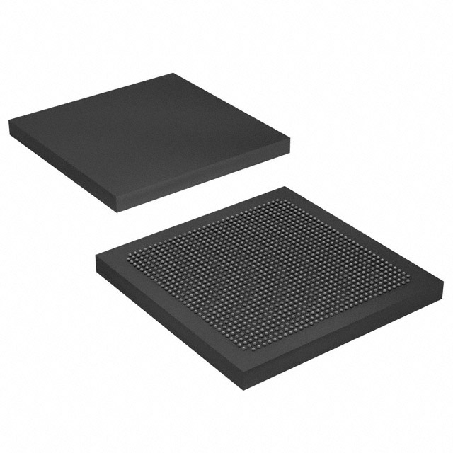
The EP2AGX190FF35C5G is an Intel Arria II GX family FPGA provided in a 1152-ball FCBGA package (35 × 35 mm) for surface-mount applications. It integrates a 40‑nm low‑power FPGA architecture with abundant logic resources, embedded memory, and I/O to address mid-to-high complexity digital designs.
Targeted at applications requiring programmable logic, DSP capability and flexible I/O, this commercial‑grade device delivers 181,165 logic elements, approximately 10.18 Mbits of embedded memory, and 612 user I/Os while operating from a core supply of 0.87 V to 0.93 V and a 0 °C to 85 °C temperature range.
Key Features
- Logic Capacity — 181,165 logic elements to implement complex combinational and sequential logic functions.
- Embedded Memory — Approximately 10.18 Mbits of on‑chip RAM for large buffering, state storage, and local data management.
- I/O Resources — 612 user I/Os supporting a wide range of single‑ended and differential signaling options in a modular I/O bank architecture.
- High‑Performance DSP — Architecture includes DSP blocks (series documentation specifies performance up to 550 MHz) and configurable multiplier options for signal processing tasks.
- Transceiver Support — Series supports high‑speed transceivers with data rates up to 6.375 Gbps and protocol circuitry for common serial interfaces.
- Programmable Logic Architecture — 40‑nm FPGA engine with adaptive logic modules and eight‑input fracturable LUTs for efficient logic packing and flexibility.
- Package & Mounting — 1152‑FBGA (35 × 35 mm) FCBGA surface mount package for dense board integration.
- Power & Temperature — Core voltage range 870 mV to 930 mV; commercial operating temperature range 0 °C to 85 °C.
- Standards & Security — Series documentation highlights integrated configuration and security features (including programming file encryption options).
- RoHS Compliant — Device is RoHS compliant.
Typical Applications
- High‑speed networking and telecom — Use the device’s high-speed transceiver support and abundant logic to implement serial protocol interfaces and packet processing.
- Digital signal processing — DSP blocks and configurable multipliers enable implementation of filters, FFTs, and other signal processing chains.
- Memory interface and buffering — Approximately 10.18 Mbits of embedded RAM and numerous I/Os support local buffering and memory controller functions.
- Custom compute and control — Large logic capacity and flexible I/O make the FPGA suitable for prototyping, hardware acceleration, and control system integration.
Unique Advantages
- Substantial logic resources: 181,165 logic elements provide the headroom to implement complex logic and state machines without immediate partitioning across devices.
- Significant embedded memory: Approximately 10.18 Mbits of on‑chip RAM reduces dependence on external memory for many buffering and storage needs.
- Flexible I/O and package density: 612 user I/Os in a 1152‑FBGA package enable dense board-level integration while preserving signal routing options.
- Series‑level high‑speed connectivity: Support for transceiver data rates up to 6.375 Gbps and common serial protocols simplifies integration of high-bandwidth links.
- Commercial grade for mainstream systems: Specified 0 °C to 85 °C operating range and RoHS compliance align with commercial application requirements.
Why Choose EP2AGX190FF35C5G?
The EP2AGX190FF35C5G combines a high logic element count with ample embedded memory and broad I/O to address demanding mid-range FPGA applications where on‑chip resources and high‑speed interfaces matter. Its 1152‑ball FCBGA package and surface‑mount compatibility make it suitable for compact board designs requiring significant programmable logic capacity.
Designed as part of the Arria II GX family, the device benefits from a documented architecture that includes DSP blocks, configurable multipliers, and transceiver support—providing a balance of performance, integration, and configurability for systems engineering and procurement.
Request a quote or submit an inquiry to receive pricing, availability, and lead‑time information for EP2AGX190FF35C5G.

























Date Founded: 1968
Headquarters: Santa Clara, California, USA
Employees: 130,000+
Revenue: $54.23 Billion
Certifications and Memberships: ISO9001:2015, ISO14001:2015, ISO17025:2017, ISO27001:2022, ISO45001:2018, ISO50001:2018


