
EP2AGX260EF29C6
| Part Description |
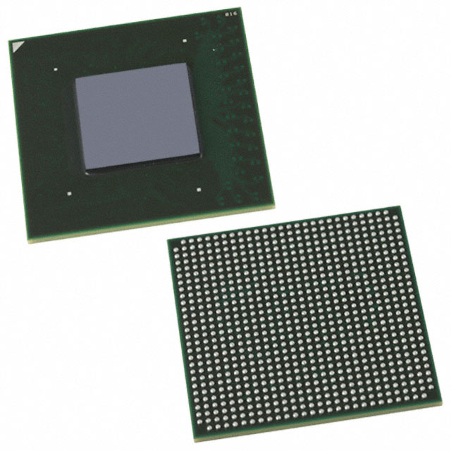
Arria II GX Field Programmable Gate Array (FPGA) IC 372 12038144 244188 780-BBGA, FCBGA |
|---|---|
| Quantity | 1,599 Available (as of June 15, 2026) |

| Product Category | Field Programmable Gate Array (FPGA) |
|---|---|
| Manufacturer | Intel |
| Manufacturing Status | Obsolete |
| Manufacturer Standard Lead Time | Contact Us |
| Datasheet |
Specifications & Environmental
| Device Package | 780-FBGA (29x29) | Grade | Commercial | Operating Temperature | 0°C – 85°C | ||
|---|---|---|---|---|---|---|---|
| Package / Case | 780-BBGA, FCBGA | Number of I/O | 372 | Voltage | 870 mV - 930 mV | ||
| Mounting Method | Surface Mount | RoHS Compliance | RoHS non-compliant | REACH Compliance | REACH Unknown | ||
| Moisture Sensitivity Level | 3 (168 Hours) | Number of LABs/CLBs | 10260 | Number of Logic Elements/Cells | 244188 | ||
| Number of Gates | N/A | ECCN | 3A001A7A | HTS Code | 8542.39.0001 | ||
| Qualification | N/A | Total RAM Bits | 12038144 |
Overview of EP2AGX260EF29C6 – Arria II GX Field Programmable Gate Array (FPGA) IC 372 12038144 244188 780-BBGA, FCBGA
The EP2AGX260EF29C6 is an Arria II GX field programmable gate array (FPGA) manufactured by Intel. It provides a high-density programmable fabric with a substantial logic resource set and embedded memory, packaged in a 780-ball FCBGA (29 × 29) surface-mount package for compact system integration.
This commercial-grade device targets applications that require large logic capacity, significant on-chip RAM, and a high I/O count while operating within a 0 °C to 85 °C ambient range and a documented core supply range of 870 mV to 930 mV.
Key Features
- Logic Capacity Approximately 244,188 logic elements for implementing complex custom logic and parallel processing functions.
- Logic Array Blocks 10,260 logic array blocks (LABs) to organize logic resources for modular and scalable design implementation.
- Embedded Memory Approximately 12.0 Mbits of on-chip RAM for high-bandwidth, low-latency storage of data and state.
- I/O Resources 372 I/O pins to support diverse interfacing requirements across multiple banks and external peripherals.
- Package & Mounting 780-ball BGA (FCBGA) package, supplier device package 780-FBGA (29×29), designed for surface-mount assembly.
- Power Supply Core voltage specified from 870 mV to 930 mV, aligning device operation to defined electrical characteristics.
- Operating Temperature & Grade Commercial grade with an operating temperature range of 0 °C to 85 °C.
- Device Documentation Device handbook and datasheet detail electrical characteristics, transceiver performance specifications, programmable I/O element (IOE) delay, and programmable output buffer delay for design and timing analysis.
- RoHS Compliance RoHS-compliant device suitable for regions and applications requiring restricted substance compliance.
Typical Applications
- High-performance digital systems Implement complex custom logic, signal processing pipelines, and control functions using the device's large logic element count and embedded memory.
- Multi-interface controllers Leverage 372 I/Os to aggregate and bridge multiple external interfaces and peripherals in a single FPGA-based controller.
- Prototyping and FPGA-based acceleration Use the Arria II GX fabric and on-chip RAM to prototype ASIC-bound logic or accelerate compute tasks where reconfigurable hardware is required.
Unique Advantages
- High logic density: Approximately 244,188 logic elements and 10,260 logic array blocks enable implementation of large, gate-rich designs without external logic expansion.
- Significant embedded memory: ~12.0 Mbits of on-chip RAM reduces dependence on external memory for many buffering and storage needs, improving system latency.
- Extensive I/O capability: 372 I/Os provide flexible interfacing options for complex systems that require many external connections.
- Compact surface-mount package: 780-ball FCBGA (29×29) package supports dense PCB layouts and reliable surface-mount assembly.
- Documented timing and transceiver details: Device handbook includes programmable I/O and output buffer delay information plus transceiver/periphery specifications to support timing closure and signal integrity planning.
- Regulatory readiness: RoHS compliance supports deployment in environments where restricted substance compliance is required.
Why Choose EP2AGX260EF29C6?
The EP2AGX260EF29C6 Arria II GX FPGA combines high logic capacity, substantial embedded memory, and a large I/O complement in a compact 780-ball FCBGA surface-mount package. Its documented electrical characteristics and device handbook coverage make it suitable for designers who need verifiable device behavior for timing, power, and transceiver considerations.
This commercial-grade device is appropriate for development and deployment in systems that operate within 0 °C to 85 °C and require a well-documented, high-density programmable platform for complex digital functions and multi-interface integration.
Request a quote or submit a product inquiry to get pricing and availability for the EP2AGX260EF29C6 Arria II GX FPGA. Our team will provide the information you need to evaluate this device for your design.


Date Founded: 1968
Headquarters: Santa Clara, California, USA
Employees: 130,000+
Revenue: $54.23 Billion
Certifications and Memberships: ISO9001:2015, ISO14001:2015, ISO17025:2017, ISO27001:2022, ISO45001:2018, ISO50001:2018


