
EP2AGX65DF25C4G
| Part Description |
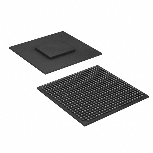
Arria II GX Field Programmable Gate Array (FPGA) IC 252 5371904 60214 572-BGA, FCBGA |
|---|---|
| Quantity | 269 Available (as of June 15, 2026) |

| Product Category | Field Programmable Gate Array (FPGA) |
|---|---|
| Manufacturer | Intel |
| Manufacturing Status | Active |
| Manufacturer Standard Lead Time | 26 Weeks |
| Datasheet |
Specifications & Environmental
| Device Package | 572-FBGA, FC (25x25) | Grade | Commercial | Operating Temperature | 0°C – 85°C | ||
|---|---|---|---|---|---|---|---|
| Package / Case | 572-BGA, FCBGA | Number of I/O | 252 | Voltage | 870 mV - 930 mV | ||
| Mounting Method | Surface Mount | RoHS Compliance | RoHS Compliant | REACH Compliance | REACH Unaffected | ||
| Moisture Sensitivity Level | 3 (168 Hours) | Number of LABs/CLBs | 2530 | Number of Logic Elements/Cells | 60214 | ||
| Number of Gates | N/A | ECCN | 3A991D | HTS Code | 8542.39.0001 | ||
| Qualification | N/A | Total RAM Bits | 5371904 |
Overview of EP2AGX65DF25C4G – Arria II GX FPGA, 60,214 logic elements, ~5.37 Mbits RAM, 252 I/Os, 572-FBGA (25×25)
The EP2AGX65DF25C4G is an Intel Arria II GX field-programmable gate array (FPGA) in a 572-FBGA package designed for commercial applications. It pairs a 40-nm, low-power FPGA engine with a high logic density and substantial embedded memory to accelerate digital signal processing, high-speed serial interfaces, and system-level integration.
Targeted at designs that require integrated DSP resources, multi-gigabit transceivers and flexible I/O, this device addresses communications, networking, storage interface, and DSP-accelerated applications while operating within a commercial temperature range.
Key Features
- FPGA Core 40-nm low-power FPGA engine with adaptive logic for efficient logic implementation.
- Logic Capacity 60,214 logic elements to implement complex programmable logic and control functions.
- Embedded Memory Approximately 5.37 Mbits of on-chip RAM for buffering, FIFOs and local data storage.
- DSP Resources High-performance DSP blocks (documented up to 550 MHz) for hardware acceleration of signal processing algorithms.
- High-speed Transceivers & Protocol Support Transceivers supporting data rates up to 6.375 Gbps with dedicated circuitry for common serial protocols including PCIe Gen1/Gen2, Ethernet, Serial RapidIO, CPRI, SDI, XAUI/RXAUI, SATA/SAS, GPON and others.
- I/O 252 user I/Os in a modular bank architecture supporting a broad range of single-ended and differential standards.
- Security & Configuration On-chip options include AES programming file encryption and parallel/serial configuration modes for design security and flexible configuration.
- Power & Supply Operates from a core voltage supply range of 870 mV to 930 mV, enabling low-voltage system designs.
- Package & Mounting Surface-mount 572-FBGA package (supplier designation 572-FBGA, FC (25×25)) for compact board-level integration.
- Operating Range & Compliance Commercial grade with an operating temperature range of 0 °C to 85 °C and RoHS compliance.
Typical Applications
- High-Speed Networking Implements multi-gigabit interfaces and protocol PHY/MAC functions for switches, routers and network appliances using the device’s transceivers and protocol support.
- Storage & Host Interfaces Enables PCIe and SATA/SAS connectivity and bridging functions where programmable logic and on-chip memory are required.
- Data Acquisition & DSP Acceleration Uses on-chip DSP blocks and embedded RAM for real-time signal processing, filtering and data aggregation in test, measurement and instrumentation systems.
- Broadcast & Video Transport Supports SD/HD/3G SDI and related serial interfaces for video transport and processing applications.
Unique Advantages
- High Logic Density: 60,214 logic elements provide capacity for complex control, protocol handling and custom logic without external ASICs.
- Significant Embedded Memory: Approximately 5.37 Mbits of on-chip RAM reduces external memory dependency for buffering and FIFOs.
- Integrated High-Speed Transceivers: Transceivers up to 6.375 Gbps and dedicated protocol circuitry simplify implementation of serial links and reduce integration time.
- DSP Acceleration: Dedicated DSP blocks (documented operation up to 550 MHz) accelerate compute-heavy signal processing tasks in hardware.
- Low-Voltage Operation: Core supply range of 870 mV to 930 mV supports power-efficient system designs.
- Commercial-Grade Reliability: Operates across 0 °C to 85 °C for standard commercial environments and is RoHS compliant.
Why Choose EP2AGX65DF25C4G?
The EP2AGX65DF25C4G positions itself as a versatile, commercially graded FPGA for designs that require a balance of logic density, embedded memory and high-speed serial connectivity. Its 40-nm low-power architecture, substantial on-chip RAM and DSP resources make it suited for communications, networking, storage interface and DSP-accelerated systems where integration and performance per watt matter.
Designed for engineers and procurement teams seeking a programmable, well-specified FPGA solution, this device offers deterministic hardware resources, integrated protocol support and a compact 572-FBGA footprint to streamline system design and reduce external component count.
Request a quote or submit an inquiry to receive pricing and availability information for the EP2AGX65DF25C4G and to begin your procurement process.


Date Founded: 1968
Headquarters: Santa Clara, California, USA
Employees: 130,000+
Revenue: $54.23 Billion
Certifications and Memberships: ISO9001:2015, ISO14001:2015, ISO17025:2017, ISO27001:2022, ISO45001:2018, ISO50001:2018


