
EP2AGX65DF25I5
| Part Description |
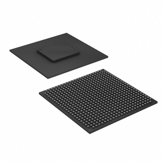
Arria II GX Field Programmable Gate Array (FPGA) IC 252 5371904 60214 572-BGA, FCBGA |
|---|---|
| Quantity | 1,361 Available (as of October 8, 2026) |
| Product Category | Field Programmable Gate Array (FPGA) |
|---|---|
| Manufacturer | Intel |
| Manufacturing Status | Obsolete |
| Manufacturer Standard Lead Time | Contact Us |
| Datasheet |
Specifications & Environmental
| Device Package | 572-FBGA, FC (25x25) | Grade | Industrial | Operating Temperature | -40°C – 100°C | ||
|---|---|---|---|---|---|---|---|
| Package / Case | 572-BGA, FCBGA | Number of I/O | 252 | Voltage | 870 mV - 930 mV | ||
| Mounting Method | Surface Mount | RoHS Compliance | RoHS non-compliant | REACH Compliance | REACH Unknown | ||
| Moisture Sensitivity Level | 3 (168 Hours) | Number of LABs/CLBs | 2530 | Number of Logic Elements/Cells | 60214 | ||
| Number of Gates | N/A | ECCN | 3A991D | HTS Code | 8542.39.0001 | ||
| Qualification | N/A | Total RAM Bits | 5371904 |
Overview of EP2AGX65DF25I5 – Arria II GX FPGA, 252 I/O, approximately 5.37 Mbits RAM, 60,214 logic elements, 572‑FBGA
The EP2AGX65DF25I5 is an Arria II GX field-programmable gate array (FPGA) offered in an industrial grade. It delivers a high-density programmable logic fabric with embedded RAM and extensive I/O, packaged in a 572‑FBGA (25 × 25) surface-mount package.
Designed for designs requiring programmable logic, on-chip memory, and configurable high-speed I/O, the device provides core voltage flexibility and an extended operating temperature range suitable for industrial environments.
Key Features
- Logic Capacity Provides 60,214 logic elements (cells) for implementing complex custom logic and control functions.
- Embedded Memory Approximately 5.37 Mbits of on-chip RAM to support buffering, lookup tables, and local storage for accelerators or protocol handling.
- I/O Count & Programmability 252 I/O pins with programmable I/O element (IOE) timing and programmable output buffer delay as described in the device family datasheet.
- Transceiver & Peripheral Support Device family datasheet documents transceiver performance and PCI Express (PIPE) HIP block support for common high-speed interface needs.
- Power and Core Supply Core supply operating range from 870 mV to 930 mV to match target power domains and system designs.
- Package & Mounting 572‑FBGA (FCBGA) package, 25 × 25 mm footprint, intended for surface-mount assembly in high-density systems.
- Industrial Grade & Thermal Range Industrial grade device with an operating temperature range of −40 °C to 100 °C for deployment in demanding ambient conditions.
- Environmental Compliance RoHS compliant.
Typical Applications
- High‑speed connectivity and protocol bridging Use transceiver performance and PCI Express (PIPE) HIP support to implement serial links, protocol bridges, and interface controllers.
- Embedded logic and acceleration Leverage 60,214 logic elements and approximately 5.37 Mbits of embedded memory for custom accelerators, data path processing, and control logic.
- Industrial control and automation Industrial-grade rating and −40 °C to 100 °C operating range enable deployment in factory automation, motor control, and field equipment.
- System integration and prototyping High I/O density and a compact 572‑FBGA package support dense board layouts and integration of multiple interfaces in development platforms.
Unique Advantages
- Substantial programmable logic: 60,214 logic elements provide the capacity needed for complex state machines, datapaths, and custom IP cores.
- Significant on‑chip memory: Approximately 5.37 Mbits of embedded RAM reduces reliance on external memory for many buffering and LUT requirements.
- Flexible I/O and high‑speed interoperability: 252 I/Os with programmable I/O timing plus documented transceiver and PCIe HIP support enable adaptable interface design.
- Industrial robustness: Rated for −40 °C to 100 °C and marked as industrial grade for applications requiring extended temperature operation.
- Compact, high‑density packaging: 572‑FBGA (25 × 25) surface-mount package supports high pin count designs in a compact footprint.
- Regulatory consideration: RoHS compliance supports designs targeting environmental regulatory requirements.
Why Choose EP2AGX65DF25I5?
The EP2AGX65DF25I5 Arria II GX FPGA combines a large logic fabric, substantial embedded memory, and extensive I/O in a compact 572‑FBGA package, making it suited for systems that need flexible, programmable hardware with industrial‑grade thermal capability. Its documented transceiver and peripheral support provides designers with the building blocks for high‑speed interfaces and protocol implementation.
Choose this device when your design requires scalable programmable logic, on‑chip memory to minimize external components, and an industrial operating range that supports deployment in demanding environments.
Request a quote or submit an inquiry to receive pricing, availability, and lead-time information for EP2AGX65DF25I5.
























Date Founded: 1968
Headquarters: Santa Clara, California, USA
Employees: 130,000+
Revenue: $54.23 Billion
Certifications and Memberships: ISO9001:2015, ISO14001:2015, ISO17025:2017, ISO27001:2022, ISO45001:2018, ISO50001:2018


