
EP2AGX95EF35I5G
| Part Description |
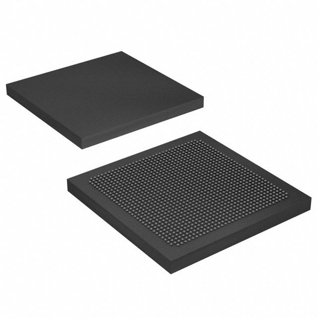
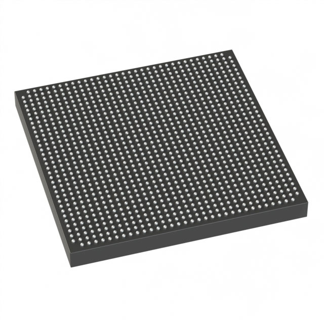
Arria II GX Field Programmable Gate Array (FPGA) IC 452 6839296 89178 1152-BBGA, FCBGA |
|---|---|
| Quantity | 410 Available (as of June 17, 2026) |

| Product Category | Field Programmable Gate Array (FPGA) |
|---|---|
| Manufacturer | Intel |
| Manufacturing Status | Active |
| Manufacturer Standard Lead Time | 26 Weeks |
| Datasheet |
Specifications & Environmental
| Device Package | 1152-FBGA (35x35) | Grade | Industrial | Operating Temperature | -40°C – 100°C | ||
|---|---|---|---|---|---|---|---|
| Package / Case | 1152-BBGA, FCBGA | Number of I/O | 452 | Voltage | 870 mV - 930 mV | ||
| Mounting Method | Surface Mount | RoHS Compliance | RoHS Compliant | REACH Compliance | REACH Unaffected | ||
| Moisture Sensitivity Level | 3 (168 Hours) | Number of LABs/CLBs | 3747 | Number of Logic Elements/Cells | 89178 | ||
| Number of Gates | N/A | ECCN | 3A991D | HTS Code | 8542.39.0001 | ||
| Qualification | N/A | Total RAM Bits | 6839296 |
Overview of EP2AGX95EF35I5G – Arria II GX FPGA, 1152‑BBGA (35×35), Industrial
The EP2AGX95EF35I5G is an Arria II GX family Field Programmable Gate Array (FPGA) in a 1152‑ball BGA package, targeted at industrial applications that require a balance of logic capacity, embedded memory and high‑speed serial connectivity. It combines a 40‑nm low‑power FPGA engine and adaptive logic modules with device‑level features from the Arria II family to support high‑bandwidth interfaces, DSP tasks and system integration.
This device provides 89,178 logic elements, approximately 6.84 Mbits of embedded memory, and 452 user I/O pins, and is specified for surface‑mount assembly with an operating range of −40 °C to 100 °C and a core supply range of 870 mV to 930 mV.
Key Features
- Core Architecture 40‑nm, low‑power FPGA engine with adaptive logic modules (ALMs) and eight‑input fracturable look‑up tables as described for the Arria II family.
- Logic Capacity 89,178 logic elements to implement complex custom logic and control functions.
- Embedded Memory Approximately 6.84 Mbits of on‑chip RAM with memory logic array blocks (MLABs) for efficient small FIFO and control‑path implementations.
- DSP and Arithmetic Family features include high‑performance DSP blocks (documented up to 550 MHz) and configurable multipliers and accumulators for signal processing and math‑intensive workloads.
- High‑Speed Serial Support The Arria II family includes transceiver technology that supports serial rates between 600 Mbps and 6.375 Gbps and physical‑layer support for common serial protocols.
- I/O and Packaging 452 device I/O pins in a 1152‑BBGA (35×35) surface‑mount package, suitable for dense board designs requiring many user I/O signals.
- Power and Voltage Core supply operating range of 870 mV to 930 mV to match platform power domains.
- Industrial Temperature Range Rated for operation from −40 °C to 100 °C for deployment in industrial environments.
- Security and Configuration Arria II family features include programmable encryption for configuration files and on‑chip termination options to simplify interface design.
- Standards and Integration Family documentation highlights integration with development tools and IP for common interfaces such as PCIe, Ethernet and memory interfaces.
Typical Applications
- High‑Speed Networking and Switches Use the device’s logic capacity, on‑chip memory and serial transceiver capability to implement packet processing, switching fabrics and line‑rate interfaces.
- PCI Express and Host Interfaces Implement PCIe and other host interfaces using the Arria II family’s physical‑layer support and embedded IP.
- Signal Processing and Video Leverage DSP blocks and configurable multipliers for video pipelines, transcoding, and real‑time signal processing tasks.
- Storage and Serial Interconnects Support serial storage protocols and high‑bandwidth interconnects using family transceiver capabilities and robust I/O.
Unique Advantages
- Highly Integrated FPGA Engine: Combines a low‑power 40‑nm FPGA fabric with ALMs and fracturable LUTs to implement dense logic with efficient resource use.
- Balanced Logic and Memory: 89,178 logic elements alongside approximately 6.84 Mbits of embedded RAM enable mixed control and data‑path designs without excessive external memory.
- High‑Speed Serial Connectivity: Family transceiver support for up to 6.375 Gbps enables implementation of modern serial protocols and high‑bandwidth links.
- Industrial Rating: Specified operation from −40 °C to 100 °C and surface‑mount packaging make the device suitable for industrial deployment.
- Platform Compatibility: Family documentation and IP support for PCIe, Ethernet and DDR3 simplify integration into conventional system architectures.
- Security and On‑Chip Features: Built‑in configuration encryption options and on‑chip termination reduce external component count and improve system security and signal integrity.
Why Choose EP2AGX95EF35I5G?
The EP2AGX95EF35I5G delivers a practical combination of logic density, embedded memory and I/O capacity in an industrial‑rated Arria II GX device. Its 40‑nm FPGA fabric and family features are suited to designs that require a balance of DSP capability, high‑speed serial links and a compact BGA package for space‑constrained boards.
This part is a fit for engineering teams building communications, industrial control, storage interface or signal‑processing systems that need field‑programmable flexibility paired with documented Arria II family features and development flow support.
Request a quote or submit an inquiry to get pricing, lead‑time and availability information for EP2AGX95EF35I5G.


Date Founded: 1968
Headquarters: Santa Clara, California, USA
Employees: 130,000+
Revenue: $54.23 Billion
Certifications and Memberships: ISO9001:2015, ISO14001:2015, ISO17025:2017, ISO27001:2022, ISO45001:2018, ISO50001:2018


