
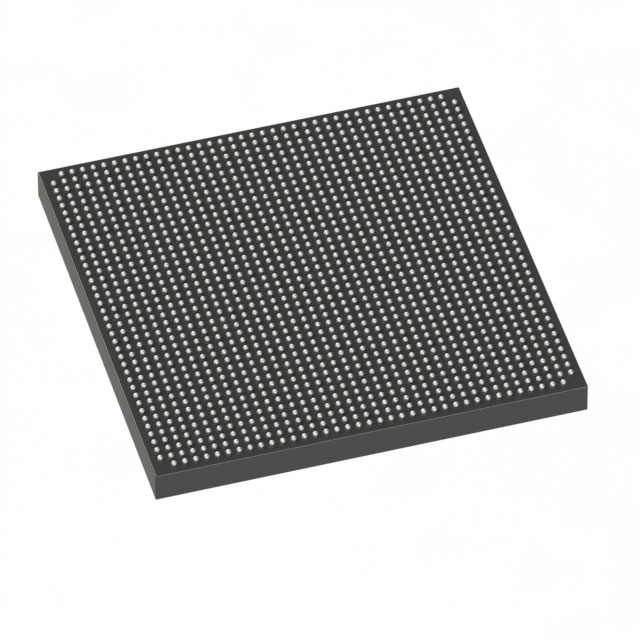
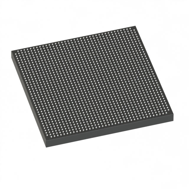
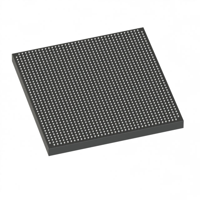
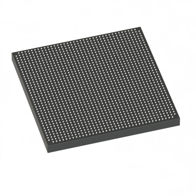
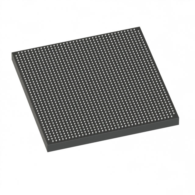
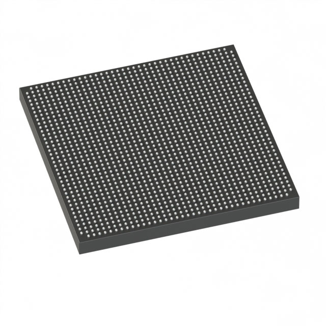
EP2AGZ300HF40I3G
| Part Description |
Field Programmable Gate Array (FPGA) IC |
|---|---|
| Quantity | 1,048 Available (as of October 8, 2026) |
| Product Category | Field Programmable Gate Array (FPGA) |
|---|---|
| Manufacturer | Intel |
| Manufacturing Status | Active |
| Manufacturer Standard Lead Time | 26 Weeks |
| Datasheet |
Specifications & Environmental
| Device Package | 1517-FBGA (40x40) | Grade | Industrial | Operating Temperature | -40°C – 100°C | ||
|---|---|---|---|---|---|---|---|
| Package / Case | 1517-BBGA, FCBGA | Number of I/O | 734 | Voltage | 870 mV - 930 mV | ||
| Mounting Method | Surface Mount | RoHS Compliance | RoHS Compliant | REACH Compliance | REACH Unaffected | ||
| Moisture Sensitivity Level | 3 (168 Hours) | Number of LABs/CLBs | 11920 | Number of Logic Elements/Cells | 298000 | ||
| Number of Gates | N/A | ECCN | N/A | HTS Code | N/A | ||
| Qualification | N/A | Total RAM Bits | 18854912 |
Overview of EP2AGZ300HF40I3G – * Field Programmable Gate Array (FPGA) IC
The EP2AGZ300HF40I3G is an Intel Arria II family FPGA featuring a 40-nm, low-power programmable logic engine designed for high-bandwidth and integration-focused designs. With a large logic capacity, substantial embedded memory, and advanced transceiver and I/O capabilities, this industrial-grade device targets communications, networking, signal processing, and other demanding embedded applications.
Built for integration with established Intel/Altera design flows and IP, the device balances performance and system-level connectivity to simplify implementation of PCIe, Ethernet, DDR3 memory interfaces and other serial protocols described for the Arria II family.
Key Features
- Core Architecture 40-nm, low-power FPGA engine from the Arria II family, optimized for programmable logic efficiency and integration with Intel design tools.
- Logic Capacity 298,000 logic elements suitable for large-scale logic integration and complex control or processing functions.
- Embedded Memory Approximately 18.85 Mbits of embedded memory for FIFOs, buffers, and on-chip data storage.
- DSP and Math Resources Family-level DSP resources (high-performance DSP blocks cited in the device family) for efficient implementation of multipliers, adders, and accumulation functions.
- High‑Speed Transceivers & Protocol Support Arria II family transceivers support data rates up to 6.375 Gbps and a wide range of serial protocols, enabling PCIe, Ethernet, Serial RapidIO, SATA, CPRI and other common physical interfaces.
- I/O and Packaging 734 user I/Os and a 1517-FBGA (40×40) / 1517-BBGA FCBGA package for dense pinout and system-level connectivity.
- Power and Voltage Core voltage supply range of 870 mV to 930 mV to match system power rails and enable predictable power budgeting.
- Industrial Temperature Range Rated for operation from −40°C to 100°C and supplied as an industrial-grade device for deployment in demanding environments.
- Security and Configuration Family features include programming file encryption (AES) and parallel/serial configuration options for design protection and flexible system boot modes.
- Compliance RoHS compliant to meet common environmental and manufacturing requirements.
Typical Applications
- High‑Bandwidth Networking Equipment Implements multi‑protocol physical layers and packet processing using integrated transceivers and abundant logic resources.
- Signal Processing and Telecom Leverages DSP blocks and on‑chip memory for real‑time filtering, encoding/decoding, and baseband processing.
- Storage and Interface Bridges Enables DDR3 memory interfaces, SATA and other high‑speed links for storage controllers and protocol bridging.
- Industrial Control and Automation Industrial temperature rating, high I/O count, and programmable logic density support advanced motor control, motion systems, and factory automation controllers.
Unique Advantages
- High Logic Density: 298,000 logic elements provide headroom for complex state machines, packet processing, and custom accelerators.
- Significant On‑Chip Memory: Approximately 18.85 Mbits of embedded RAM reduces external memory dependency for buffering and local data storage.
- Robust Serial Connectivity: Family transceivers rated up to 6.375 Gbps support modern high‑speed serial protocols for flexible system interfacing.
- Extensive I/O Count: 734 user I/Os in a compact FBGA package enable dense board integration and diverse peripheral interfacing.
- Industrial Reliability: Industrial grade device with −40°C to 100°C operating range for reliable field deployment in harsh environments.
- Design Flow and IP Ecosystem: Designed to integrate with Intel/Altera tools and IP libraries to accelerate development of common interfaces and subsystems.
Why Choose EP2AGZ300HF40I3G?
The EP2AGZ300HF40I3G combines high logic capacity, ample embedded memory, and comprehensive I/O/transceiver resources in an industrial‑rated Arria II FPGA package. It is well suited for engineers designing high‑throughput communications, signal processing, and industrial control systems that require on-chip processing, flexible interface support, and predictable operating margins.
Backed by Intel’s Arria II family documentation and toolchain integration, this device offers a scalable platform for mid-to-large FPGA designs where integration, connectivity, and industrial operating range are priorities.
Request a quote or submit an inquiry to receive pricing, availability, and additional technical support for the EP2AGZ300HF40I3G.





















Date Founded: 1968
Headquarters: Santa Clara, California, USA
Employees: 130,000+
Revenue: $54.23 Billion
Certifications and Memberships: ISO9001:2015, ISO14001:2015, ISO17025:2017, ISO27001:2022, ISO45001:2018, ISO50001:2018


