
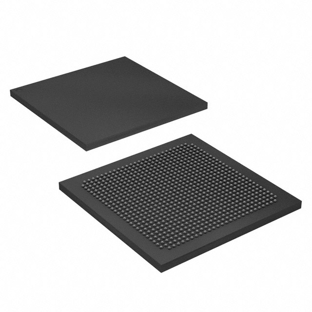
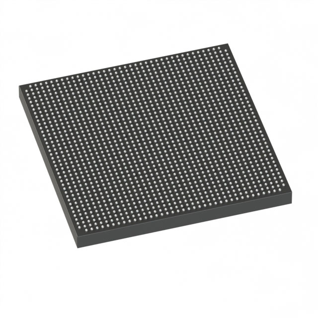
EP2AGZ300HF40C4G
| Part Description |
Field Programmable Gate Array (FPGA) IC |
|---|---|
| Quantity | 643 Available (as of June 10, 2026) |

| Product Category | Field Programmable Gate Array (FPGA) |
|---|---|
| Manufacturer | Intel |
| Manufacturing Status | Active |
| Manufacturer Standard Lead Time | 26 Weeks |
| Datasheet |
Specifications & Environmental
| Device Package | 1517-FBGA (40x40) | Grade | Commercial | Operating Temperature | 0°C – 85°C | ||
|---|---|---|---|---|---|---|---|
| Package / Case | 1517-BBGA, FCBGA | Number of I/O | 734 | Voltage | 870 mV - 930 mV | ||
| Mounting Method | Surface Mount | RoHS Compliance | RoHS Compliant | REACH Compliance | REACH Unaffected | ||
| Moisture Sensitivity Level | 3 (168 Hours) | Number of LABs/CLBs | 11920 | Number of Logic Elements/Cells | 298000 | ||
| Number of Gates | N/A | ECCN | N/A | HTS Code | N/A | ||
| Qualification | N/A | Total RAM Bits | 18854912 |
Overview of EP2AGZ300HF40C4G – Field Programmable Gate Array (FPGA) IC
The EP2AGZ300HF40C4G is an Intel Arria II family Field Programmable Gate Array (FPGA) IC optimized for commercial-grade embedded and interface applications. It combines a 40-nm low-power programmable logic engine with high I/O density and on-chip memory to support high-bandwidth system integration and protocol implementation.
Key Features
- Core Architecture 40-nm Arria II device family architecture with a low-power programmable logic engine designed for ease of use and integration.
- Logic Capacity 298,000 logic elements and 11,920 logic blocks provide substantial combinational and sequential resources for complex designs.
- Embedded Memory Approximately 18.85 Mbits of on-chip RAM for buffering, FIFOs, and local data storage.
- I/O and Transceivers 734 user I/O pins and family-level support for up to 24 full‑duplex CDR-based transceivers with serial rates up to 6.375 Gbps enable dense, high-speed connectivity and protocol support.
- DSP and Math Resources Family features include high-performance DSP blocks capable of supporting heavy signal processing tasks and configurable multiplier widths for flexible arithmetic implementations.
- Power and Voltage Core supply range of 0.870 V to 0.930 V with architecture-level power-optimization techniques for lower overall system power.
- Package & Mounting 1517-FBGA (40 × 40) FCBGA package in a surface-mount form factor for board-level integration.
- Operating Range & Grade Commercial grade device specified for 0 °C to 85 °C operation.
- Security & Configuration Family-level design security includes support for 256-bit AES programming file encryption and multiple configuration options.
- Environmental Compliance RoHS compliant.
Typical Applications
- High‑Bandwidth Networking Implements interfacing and protocol logic for Ethernet and PCI Express systems using high I/O density and transceiver support.
- Storage & Serial Interfaces Supports SATA/SAS and other serial storage protocols with on-chip transceiver and SERDES capability.
- Video and Broadcast Processing Handles SD/HD/3G SDI and other serial digital interfaces with embedded memory and DSP resources for real‑time processing.
- Wireless & Infrastructure Suitable for front-end interface and transport protocols (for example CPRI, OBSAI) where deterministic I/O and transceiver performance are required.
- DSP Acceleration Offloads compute-intensive signal processing tasks using dedicated DSP blocks and on-chip memory.
Unique Advantages
- High logic and memory density: Large logic element count and approximately 18.85 Mbits of embedded RAM reduce the need for external memory and simplify system architecture.
- Broad interface support: High I/O count and family-level transceiver capability enable integration of multiple high-speed serial and parallel interfaces on a single device.
- Power-efficient 40-nm engine: Low-voltage core operation and architecture-level power optimizations help lower system power consumption.
- Commercial-grade reliability: Specified for 0 °C to 85 °C operation and supplied in a compact FCBGA package for robust board-level integration.
- Design security and configuration options: Supported programming/encryption features guard intellectual property and support secure deployment.
- Software and IP ecosystem: Arria II family integration with vendor IP and development tools simplifies implementation of common interfaces and accelerates time to market.
Why Choose EP2AGZ300HF40C4G?
The EP2AGZ300HF40C4G balances substantial logic capacity, on-chip memory, and high I/O density in a commercial-grade Arria II FPGA package, making it well suited for designs that require integrated high‑bandwidth interfaces and on‑device signal processing. Its 40-nm low-power architecture and configurable DSP features give teams flexibility to implement complex protocol stacks and acceleration blocks while managing board-level power and footprint.
Targeted at embedded systems, networking, video, storage, and DSP-accelerated applications, this device offers a platform-level feature set and vendor tooling to support scalable designs and long-term project needs.
Request a quote or submit an inquiry to obtain pricing, availability, and additional technical support for EP2AGZ300HF40C4G.


Date Founded: 1968
Headquarters: Santa Clara, California, USA
Employees: 130,000+
Revenue: $54.23 Billion
Certifications and Memberships: ISO9001:2015, ISO14001:2015, ISO17025:2017, ISO27001:2022, ISO45001:2018, ISO50001:2018


