
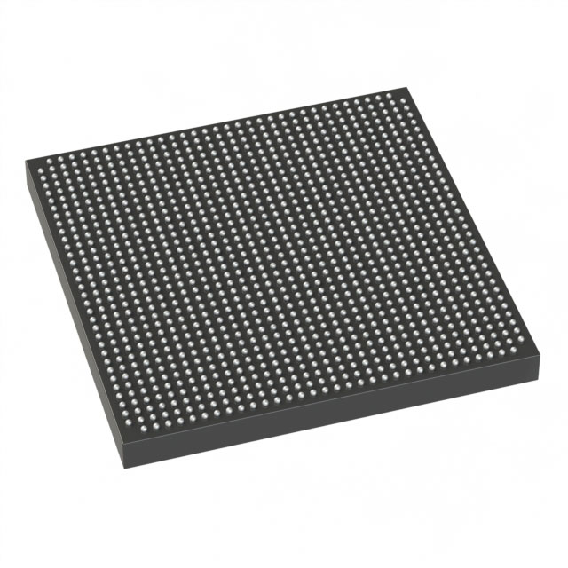
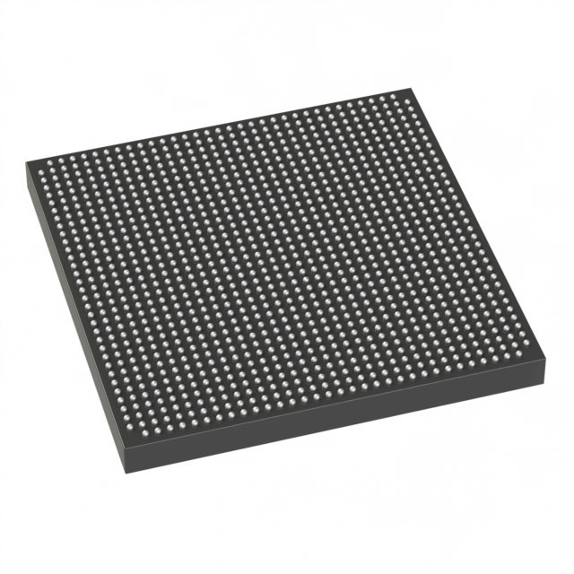
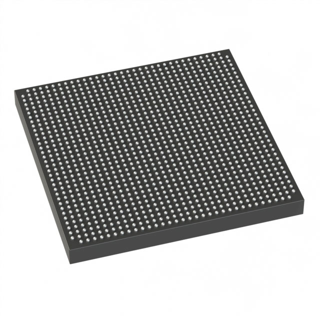
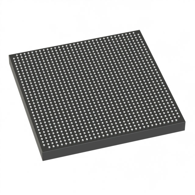
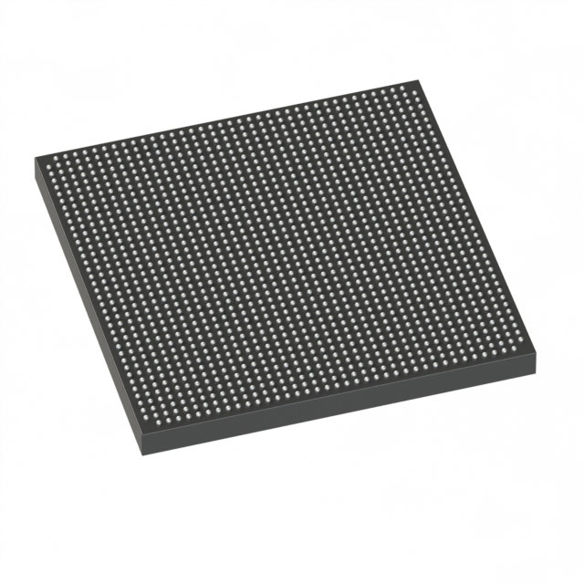
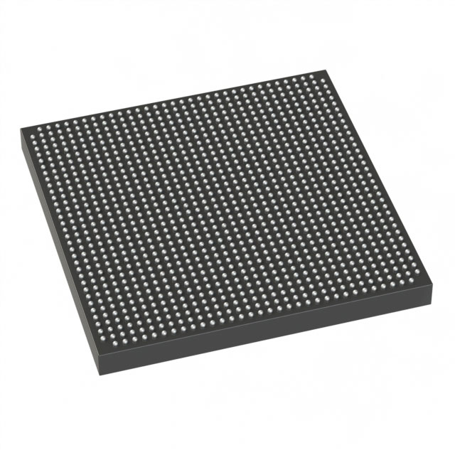
EP2AGZ350FF35C3G
| Part Description |
Field Programmable Gate Array (FPGA) IC |
|---|---|
| Quantity | 122 Available (as of October 7, 2026) |
| Product Category | Field Programmable Gate Array (FPGA) |
|---|---|
| Manufacturer | Intel |
| Manufacturing Status | Active |
| Manufacturer Standard Lead Time | 26 Weeks |
| Datasheet |
Specifications & Environmental
| Device Package | 1152-FBGA (35x35) | Grade | Commercial | Operating Temperature | 0°C – 85°C | ||
|---|---|---|---|---|---|---|---|
| Package / Case | 1152-BBGA, FCBGA | Number of I/O | 554 | Voltage | 870 mV - 930 mV | ||
| Mounting Method | Surface Mount | RoHS Compliance | RoHS Compliant | REACH Compliance | REACH Unaffected | ||
| Moisture Sensitivity Level | 3 (168 Hours) | Number of LABs/CLBs | 13940 | Number of Logic Elements/Cells | 348500 | ||
| Number of Gates | N/A | ECCN | N/A | HTS Code | N/A | ||
| Qualification | N/A | Total RAM Bits | 21270528 |
Overview of EP2AGZ350FF35C3G – Field Programmable Gate Array (FPGA) IC
The EP2AGZ350FF35C3G is an Intel Arria II family FPGA device offering a 40‑nm, low‑power programmable logic engine tailored for designs that require substantial logic capacity, embedded memory and high‑speed serial interfaces. Its architecture supports integration of DSP functions, memory interfaces and serial protocols, making it suitable for communications, video transport, signal processing and high‑bandwidth embedded systems.
This commercial‑grade, surface‑mount FCBGA device combines a large logic fabric with significant on‑chip RAM and extensive I/O to help designers implement complex, multi‑function systems while leveraging family features such as on‑chip termination, configuration security and high‑speed transceiver support.
Key Features
- Core Architecture 40‑nm low‑power FPGA engine from the Arria II family with adaptive logic modules and eight‑input fracturable LUTs to support efficient logic implementation.
- Logic Capacity 348,500 logic elements for implementing large or highly parallel designs.
- Embedded Memory Approximately 21.27 Mbits of embedded memory (21,270,528 total RAM bits) to support buffers, FIFOs and on‑chip storage.
- DSP and Math Resources Family DSP blocks suitable for high‑performance signal processing tasks; Arria II devices include optimized multipliers and accumulator functions.
- High‑Speed Transceivers Family support for multi‑Gbps transceivers operating up to 6.375 Gbps, enabling implementation of serial protocols and high‑bandwidth links.
- I/O and Interface Density 554 user I/Os to connect parallel interfaces, memory buses and mixed signal front ends.
- Package and Mounting 1152‑FBGA package (35 × 35 mm) in a surface‑mount FCBGA/BBGA form factor for board‑level integration.
- Power and Voltage Core voltage supply range of 870 mV to 930 mV for the device core.
- Operating Environment Commercial grade with an operating temperature range of 0 °C to 85 °C.
- Security and Configuration Family features include 256‑bit AES programming file encryption and multiple configuration options for design security and flexible deployment.
- Compliance RoHS compliant for restrictions on hazardous substances.
Typical Applications
- Communications Infrastructure Implement high‑bandwidth line cards, protocol bridging and serial links using on‑chip transceivers and large logic capacity.
- Video and Broadcast Process and transport SD/HD/3G signals and other high‑speed media streams leveraging the device’s transceiver and DSP capabilities.
- High‑Performance Embedded Systems Offload compute‑intensive tasks and implement custom accelerators using the extensive logic fabric and embedded memory.
- Memory Interface and Aggregation Integrate DDR3 and other memory interfaces alongside custom logic and buffering using available on‑chip RAM.
Unique Advantages
- High Logic Density: 348,500 logic elements provide headroom for complex state machines, protocol stacks and parallel datapaths, reducing the need for multiple devices.
- Substantial On‑Chip Memory: Approximately 21.27 Mbits of embedded RAM minimize external memory dependence for buffering and small‑FIFO implementations.
- Broad Interface Support: Family transceiver capability up to 6.375 Gbps and 554 I/Os simplify integration of high‑speed serial links and parallel buses.
- Security and Flexible Configuration: Integrated AES programming file encryption and multiple configuration modes support secure deployment and update workflows.
- Commercial‑Grade Reliability: Specified for 0 °C to 85 °C operation and supplied in a robust FCBGA package for surface‑mount assembly.
- Regulatory Compliance: RoHS compliance supports environmental and manufacturing requirements.
Why Choose EP2AGZ350FF35C3G?
The EP2AGZ350FF35C3G delivers a balanced combination of logic capacity, embedded memory and high‑speed interface support drawn from the Arria II family architecture. It is positioned for engineers who need to implement substantive FPGA‑based functions—such as protocol offload, DSP acceleration and high‑bandwidth I/O—within a single, commercially rated device.
With a large I/O count, a high logic element tally and family features like transceiver support and configuration security, this device is well suited to mid‑to high‑complexity designs that require integration, scalability and predictable performance backed by Intel’s Arria II device capabilities.
Request a quote or submit a request for pricing and availability for EP2AGZ350FF35C3G today.





















Date Founded: 1968
Headquarters: Santa Clara, California, USA
Employees: 130,000+
Revenue: $54.23 Billion
Certifications and Memberships: ISO9001:2015, ISO14001:2015, ISO17025:2017, ISO27001:2022, ISO45001:2018, ISO50001:2018


