
EP2S30F672C3
| Part Description |
Stratix® II Field Programmable Gate Array (FPGA) IC 500 1369728 33880 672-BBGA |
|---|---|
| Quantity | 209 Available (as of June 15, 2026) |

| Product Category | Field Programmable Gate Array (FPGA) |
|---|---|
| Manufacturer | Intel |
| Manufacturing Status | Obsolete |
| Manufacturer Standard Lead Time | Contact Us |
| Datasheet |
Specifications & Environmental
| Device Package | 672-FBGA (27x27) | Grade | Commercial | Operating Temperature | 0°C – 85°C | ||
|---|---|---|---|---|---|---|---|
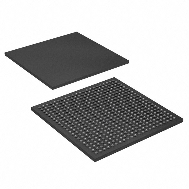
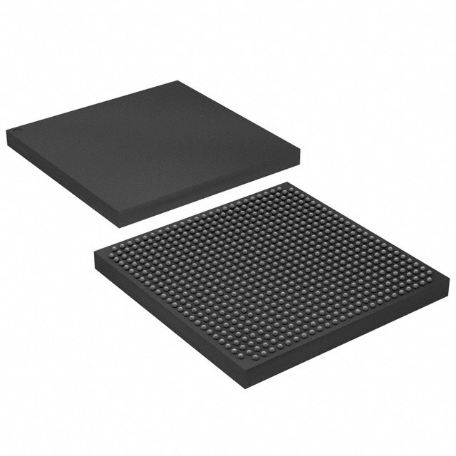
| Package / Case | 672-BBGA | Number of I/O | 500 | Voltage | 1.15 V - 1.25 V | ||
| Mounting Method | Surface Mount | RoHS Compliance | RoHS non-compliant | REACH Compliance | REACH Unaffected | ||
| Moisture Sensitivity Level | 3 (168 Hours) | Number of LABs/CLBs | 1694 | Number of Logic Elements/Cells | 33880 | ||
| Number of Gates | N/A | ECCN | 3A001A7A | HTS Code | 8542.39.0001 | ||
| Qualification | N/A | Total RAM Bits | 1369728 |
Overview of EP2S30F672C3 – Stratix® II FPGA, 33,880 LEs, 672‑BBGA
The EP2S30F672C3 is a Stratix® II Field Programmable Gate Array (FPGA) in a 672‑BBGA package from Intel. It combines a large logic fabric with embedded memory, dedicated DSP and clocking resources, and a dense I/O complement to address designs that require programmable logic, signal processing blocks, and complex I/O interfacing.
Key on‑device resources include 33,880 logic elements implemented across 1,694 LABs, approximately 1.37 Mbits of embedded RAM, and up to 500 user I/O pins — all in a surface‑mount 672‑ball FBGA (27×27) footprint. The device operates from a 1.15 V–1.25 V core supply and is specified for commercial temperature operation (0 °C to 85 °C).
Key Features
- Core logic — 33,880 logic elements arranged across 1,694 LABs provide the programmable fabric for glue logic, state machines, and custom datapaths.
- Embedded memory — Approximately 1.37 Mbits (1,369,728 bits) of on‑chip RAM for FIFOs, buffers, and intermediate storage.
- DSP & clocking — Device family includes dedicated digital signal processing blocks and enhanced/fast PLLs and clock networks to support synchronous datapaths and mixed clock domains.
- I/O architecture — Up to 500 I/O pins with high‑speed differential and double‑data‑rate I/O support and advanced I/O standard options as described in the Stratix II device documentation.
- Configuration and debug — Supports standard configuration schemes and on‑chip debug features referenced in the Stratix II device handbook (SignalTap II, JTAG boundary‑scan).
- Power and mounting — Surface‑mount 672‑BBGA package (supplier package: 672‑FBGA, 27×27); core supply range 1.15 V–1.25 V.
- Operating conditions & compliance — Commercial grade operation from 0 °C to 85 °C and RoHS compliant.
Typical Applications
- High‑speed memory interfaces — Utilize the device’s I/O architecture and embedded memory for external RAM interfacing and memory buffering tasks.
- Signal processing and DSP acceleration — Dedicated DSP blocks and on‑chip RAM enable implementation of fixed and streaming signal processing pipelines.
- Protocol bridging and interface aggregation — Dense I/O (up to 500 pins) supports protocol conversion, multi‑lane interfaces, and high‑density connectivity.
- Custom logic and prototyping — Large logic capacity and comprehensive configuration/debug options make the device suitable for complex custom logic, control, and prototyping roles.
Unique Advantages
- High logic capacity: 33,880 logic elements across 1,694 LABs enable implementation of large finite‑state machines, control logic, and parallel datapaths without external glue logic.
- Substantial embedded memory: Approximately 1.37 Mbits of on‑chip RAM reduces dependence on external memory for buffering and temporary storage.
- Dense and flexible I/O: Up to 500 I/Os in a 672‑BBGA package supports complex multi‑interface designs and high pin‑count requirements in a compact footprint.
- Targeted DSP and timing resources: Dedicated DSP blocks plus enhanced PLLs and clock networks provide building blocks for synchronized, high‑throughput signal paths.
- Commercial temperature and RoHS compliant: Specified for 0 °C to 85 °C operation and RoHS compliance for broad deployment in commercial applications.
- Standard core voltage: 1.15 V–1.25 V core supply simplifies integration with common FPGA power rail architectures.
Why Choose EP2S30F672C3?
The EP2S30F672C3 delivers a balanced combination of logic capacity, embedded memory, DSP resources, and dense I/O in a compact 672‑BBGA package. It is well suited for designs that require significant on‑chip resources for signal processing, protocol handling, and complex control logic while remaining within commercial temperature and power envelopes.
Backed by the Stratix II device handbook and the device family’s documented architecture (logic array blocks, TriMatrix memory organization, DSP blocks, PLLs, and I/O structures), this part is appropriate for engineers seeking a documented, programmable solution for medium‑to‑large FPGA designs.
Request a quote or submit a product inquiry for EP2S30F672C3 to obtain pricing and availability for your next design.


Date Founded: 1968
Headquarters: Santa Clara, California, USA
Employees: 130,000+
Revenue: $54.23 Billion
Certifications and Memberships: ISO9001:2015, ISO14001:2015, ISO17025:2017, ISO27001:2022, ISO45001:2018, ISO50001:2018


