
EP2S30F672C3N
| Part Description |
Stratix® II Field Programmable Gate Array (FPGA) IC 500 1369728 33880 672-BBGA |
|---|---|
| Quantity | 380 Available (as of June 14, 2026) |

| Product Category | Field Programmable Gate Array (FPGA) |
|---|---|
| Manufacturer | Intel |
| Manufacturing Status | Obsolete |
| Manufacturer Standard Lead Time | Contact Us |
| Datasheet |
Specifications & Environmental
| Device Package | 672-FBGA (27x27) | Grade | Commercial | Operating Temperature | 0°C – 85°C | ||
|---|---|---|---|---|---|---|---|
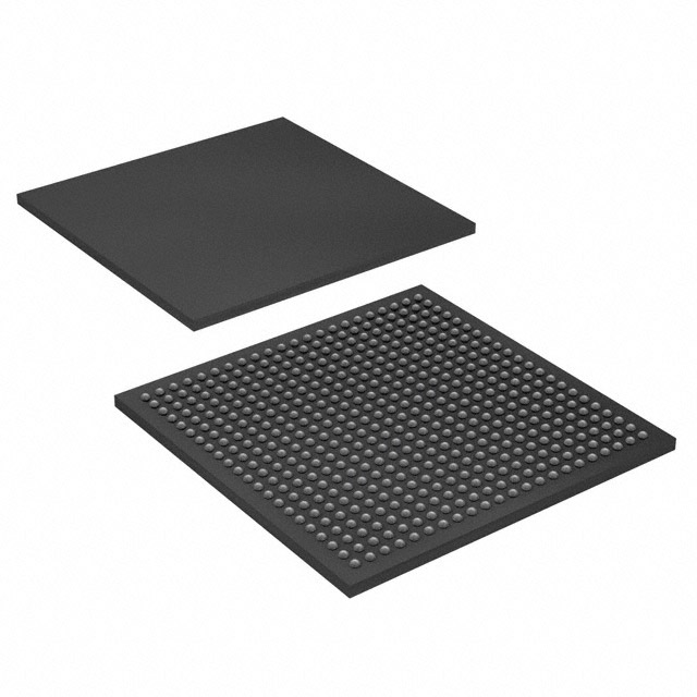
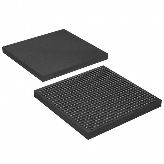
| Package / Case | 672-BBGA | Number of I/O | 500 | Voltage | 1.15 V - 1.25 V | ||
| Mounting Method | Surface Mount | RoHS Compliance | RoHS Compliant | REACH Compliance | REACH Unaffected | ||
| Moisture Sensitivity Level | 3 (168 Hours) | Number of LABs/CLBs | 1694 | Number of Logic Elements/Cells | 33880 | ||
| Number of Gates | N/A | ECCN | 3A991D | HTS Code | 8542.39.0001 | ||
| Qualification | N/A | Total RAM Bits | 1369728 |
Overview of EP2S30F672C3N – Stratix® II FPGA, 500 I/O, ~1.37 Mbits, 33,880 Logic Elements
The EP2S30F672C3N is a Stratix® II field-programmable gate array (FPGA) in a 672-BBGA surface-mount package. It delivers a programmable logic platform with 33,880 logic elements, approximately 1.37 Mbits of embedded memory, and up to 500 I/O pins for complex system integration.
Designed for commercial-grade applications, this device operates from a core supply range of 1.15 V to 1.25 V and supports an ambient operating temperature range of 0 °C to 85 °C. The Stratix II architecture documented in the device handbook provides on-chip resources such as PLLs, dedicated DSP blocks, multi-track interconnect, and advanced I/O capabilities for timing- and interface-critical designs.
Key Features
- Programmable Logic — 33,880 logic elements to implement complex digital functions and state machines.
- Embedded Memory — Approximately 1.37 Mbits of on-chip RAM for buffering, FIFOs, and data storage within user logic.
- I/O Capacity — Up to 500 I/O pins supporting a wide range of interfacing and parallel/serial connectivity needs.
- Power and Temperature — Core voltage supply between 1.15 V and 1.25 V; commercial operating temperature range 0 °C to 85 °C.
- Package & Mounting — 672-BBGA package; supplier device package listed as 672-FBGA (27×27 mm) for surface-mount board designs.
- Clocking & Timing — Architecture includes PLLs and hierarchical clock networks for flexible clock distribution and timing control.
- DSP & Memory Architecture — Dedicated digital signal processing block and TriMatrix memory organization for efficient signal processing and memory access.
- Advanced I/O Support — High-speed I/O features, DDR pin support, on‑chip termination options, and programmable I/O standards as described in the device handbook.
- Design & Test Support — JTAG boundary-scan, embedded logic analysis, configuration and testing features documented in the Stratix II handbook.
- RoHS Compliant — Device is compliant with RoHS environmental regulations.
Typical Applications
- High-speed data path and interface bridging — Use the device’s advanced I/O and PLL clocking to implement high-bandwidth interfaces and protocol bridging where flexible pinouts and timing control are required.
- Signal processing — Leverage the dedicated DSP block and embedded RAM for data filtering, transformation, and real-time stream processing tasks.
- External memory controllers — Utilize DDR I/O support and on-chip memory structures for external RAM interfacing and memory controller implementations.
- Custom logic and state machines — Implement complex control, sequencing, and glue logic across a wide range of commercial electronic systems using the 33,880 logic elements.
Unique Advantages
- Large logic capacity: 33,880 logic elements provide substantial programmable resources for integration of multiple functions on a single device.
- Integrated memory footprint: Approximately 1.37 Mbits of embedded RAM reduce external memory needs for many buffering and storage tasks.
- High I/O density: Up to 500 I/O pins enable extensive peripheral and bus connectivity without immediate need for external multiplexing.
- Flexible clocking: On-chip PLLs and hierarchical clock networks support complex timing regimes and multi-clock domain designs.
- Commercial-grade reliability: Specified operating range (0 °C to 85 °C) and RoHS compliance align with standard commercial product requirements.
- Surface-mount, compact package: 672-BBGA / 672-FBGA (27×27 mm) packaging suits dense board layouts and production assembly processes.
Why Choose EP2S30F672C3N?
The EP2S30F672C3N positions itself as a versatile Stratix II FPGA option for commercial electronic designs that require substantial programmable logic, embedded memory, and high I/O counts. Its documented architecture—covering PLLs, DSP blocks, multi-track interconnect, and advanced I/O features—supports implementations ranging from interface bridging to real-time signal processing.
For design teams and procurement seeking a field-programmable platform with a proven architecture and detailed device handbook support, this FPGA delivers a balanced combination of capacity, on-chip resources, and clear electrical and thermal operating parameters for predictable integration into commercial systems.
Request a quote or submit an inquiry to receive pricing and availability information for EP2S30F672C3N. Our team can provide technical and logistical details to help you evaluate this Stratix II FPGA for your next design.


Date Founded: 1968
Headquarters: Santa Clara, California, USA
Employees: 130,000+
Revenue: $54.23 Billion
Certifications and Memberships: ISO9001:2015, ISO14001:2015, ISO17025:2017, ISO27001:2022, ISO45001:2018, ISO50001:2018


