
EP2S30F672C4
| Part Description |
Stratix® II Field Programmable Gate Array (FPGA) IC 500 1369728 33880 672-BBGA |
|---|---|
| Quantity | 1,732 Available (as of June 15, 2026) |

| Product Category | Field Programmable Gate Array (FPGA) |
|---|---|
| Manufacturer | Intel |
| Manufacturing Status | Obsolete |
| Manufacturer Standard Lead Time | Contact Us |
| Datasheet |
Specifications & Environmental
| Device Package | 672-FBGA (27x27) | Grade | Commercial | Operating Temperature | 0°C – 85°C | ||
|---|---|---|---|---|---|---|---|
| Package / Case | 672-BBGA | Number of I/O | 500 | Voltage | 1.15 V - 1.25 V | ||
| Mounting Method | Surface Mount | RoHS Compliance | RoHS non-compliant | REACH Compliance | REACH Unaffected | ||
| Moisture Sensitivity Level | 3 (168 Hours) | Number of LABs/CLBs | 1694 | Number of Logic Elements/Cells | 33880 | ||
| Number of Gates | N/A | ECCN | 3A001A7A | HTS Code | 8542.39.0001 | ||
| Qualification | N/A | Total RAM Bits | 1369728 |
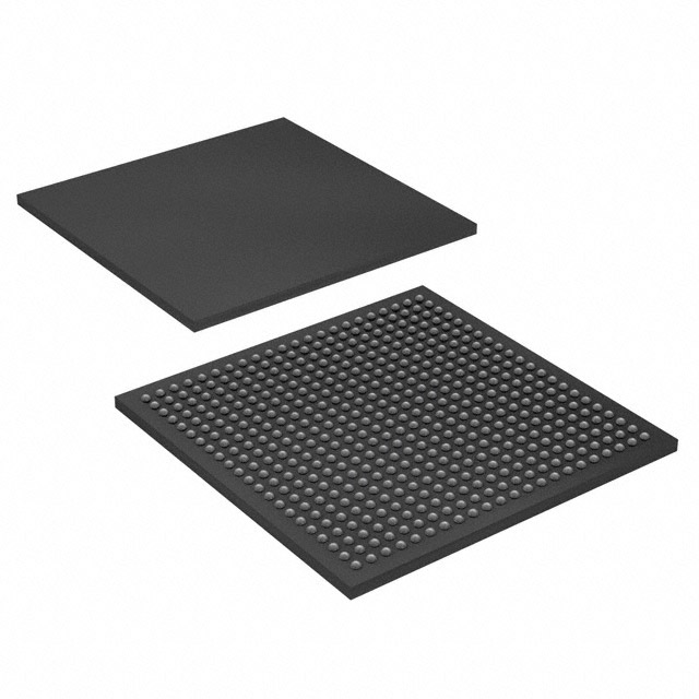
Overview of EP2S30F672C4 – Stratix II FPGA, 33,880 logic elements, 672-BBGA
The EP2S30F672C4 is an Intel Stratix® II field-programmable gate array (FPGA) in a 672-ball BGA package designed for commercial-grade embedded and communications applications. It combines a high count of logic elements and logic array blocks with substantial on-chip RAM and a large I/O complement to support complex digital designs.
Built around the Stratix II architecture, this device targets designs that require dense logic, integrated memory resources, flexible I/O, and on-chip DSP/clocking capabilities as documented in the Stratix II device handbook and datasheet.
Key Features
- Core Logic 33,880 logic elements implemented across 1,694 LABs (logic array blocks) to support complex combinational and sequential logic designs.
- Embedded Memory Approximately 1.37 Mbits of on-chip RAM for data buffering, FIFOs, and lookup tables.
- I/O Capacity 500 user I/O pins to support wide parallel interfaces and multiple peripheral connections; I/O structure and standards are detailed in the Stratix II handbook.
- DSP and Clocking Resources Dedicated digital signal processing blocks and enhanced/fast PLLs are part of the Stratix II architecture to support signal processing, clock management, and multi-clock-domain designs (see device handbook).
- Configuration & Debug IEEE 1149.1 JTAG boundary-scan support and embedded logic analyzer capabilities (SignalTap II) are included in the Stratix II documentation for configuration and in-system debug.
- Power and Supply Core voltage supply range of 1.15 V to 1.25 V, enabling defined power-domain design and integration.
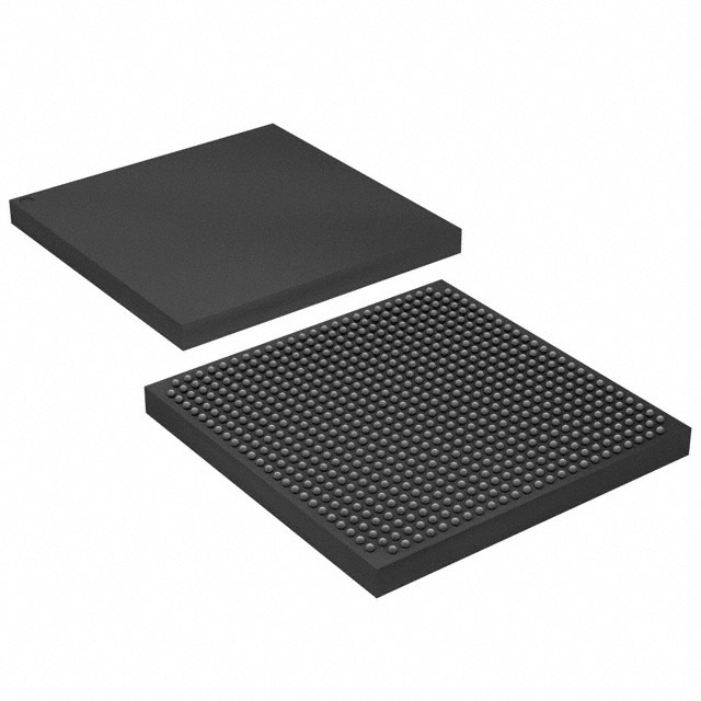
- Package & Mounting Surface-mount 672-BBGA package (supplier package listed as 672-FBGA, 27×27) suitable for high-density board designs.
- Operating Range & Compliance Commercial-grade device with an operating temperature range of 0 °C to 85 °C and RoHS compliance.
Typical Applications
- Communications Equipment Interfaces and protocol processing where high I/O counts and on-chip memory support external memory interfacing and multi-channel data paths.
- Signal Processing DSP-oriented designs that leverage the device's embedded DSP blocks, PLLs, and internal RAM for filtering, transforms, and real-time processing.
- Embedded Control Systems Custom control logic and glue logic for industrial and commercial embedded systems requiring dense logic integration and abundant I/O.
- Prototyping & Platform Development Hardware platforms and proof-of-concept systems that benefit from reprogrammability, on-chip debug (SignalTap II), and JTAG support for iterative development.
Unique Advantages
- High logic density: 33,880 logic elements and 1,694 LABs provide the capacity to implement large-scale custom logic and complex state machines.
- Substantial embedded memory: Approximately 1.37 Mbits of on-chip RAM reduces dependence on external memory for many buffering and LUT requirements.
- Extensive I/O: 500 I/O pins accommodate wide buses, parallel interfaces, and multiple peripheral connections without extensive external multiplexing.
- Integrated DSP and clocking: Stratix II DSP blocks and PLL resources (documented in the device handbook) enable efficient implementation of high-throughput signal-processing chains and precise clock domains.
- Design and debug support: Built-in JTAG boundary-scan and SignalTap II embedded logic analyzer capabilities facilitate configuration, testing, and in-system debug workflows.
- Commercial-ready packaging and compliance: 672-BBGA (27×27 FBGA footprint) surface-mount package with RoHS compliance for standard commercial applications.
Why Choose EP2S30F672C4?
The EP2S30F672C4 positions itself as a high-density Stratix II FPGA option for commercial designs that require a balance of logic capacity, embedded memory, and extensive I/O. Its combination of 33,880 logic elements, dedicated DSP and clocking resources, and nearly 1.37 Mbits of on-chip RAM makes it suitable for communications, signal processing, and complex embedded control applications.
Engineers selecting this device benefit from the Stratix II architecture documented in the device handbook—covering logic array structure, memory organization, I/O features, and configuration/debug capabilities—delivering a well-documented platform for scalable, reprogrammable hardware solutions.
Request a quote or submit an inquiry for EP2S30F672C4 to receive pricing and availability information tailored to your project requirements.


Date Founded: 1968
Headquarters: Santa Clara, California, USA
Employees: 130,000+
Revenue: $54.23 Billion
Certifications and Memberships: ISO9001:2015, ISO14001:2015, ISO17025:2017, ISO27001:2022, ISO45001:2018, ISO50001:2018


