
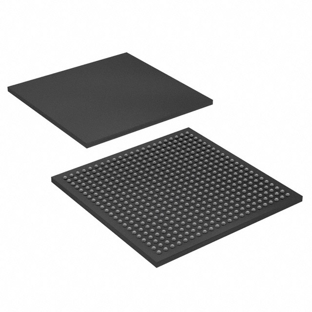
EP2S60F484C5
| Part Description |
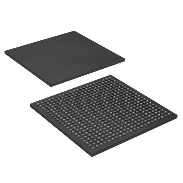
Stratix® II Field Programmable Gate Array (FPGA) IC 334 2544192 60440 484-BBGA |
|---|---|
| Quantity | 1,918 Available (as of October 7, 2026) |
| Product Category | Field Programmable Gate Array (FPGA) |
|---|---|
| Manufacturer | Intel |
| Manufacturing Status | Obsolete |
| Manufacturer Standard Lead Time | Contact Us |
| Datasheet |
Specifications & Environmental
| Device Package | 484-FBGA (23x23) | Grade | Commercial | Operating Temperature | 0°C – 85°C | ||
|---|---|---|---|---|---|---|---|
| Package / Case | 484-BBGA | Number of I/O | 334 | Voltage | 1.15 V - 1.25 V | ||
| Mounting Method | Surface Mount | RoHS Compliance | RoHS non-compliant | REACH Compliance | REACH Unaffected | ||
| Moisture Sensitivity Level | 3 (168 Hours) | Number of LABs/CLBs | 3022 | Number of Logic Elements/Cells | 60440 | ||
| Number of Gates | N/A | ECCN | 3A001A7A | HTS Code | 8542.39.0001 | ||
| Qualification | N/A | Total RAM Bits | 2544192 |
Overview of EP2S60F484C5 – Stratix® II Field Programmable Gate Array (FPGA) IC 334 2544192 60440 484-BBGA
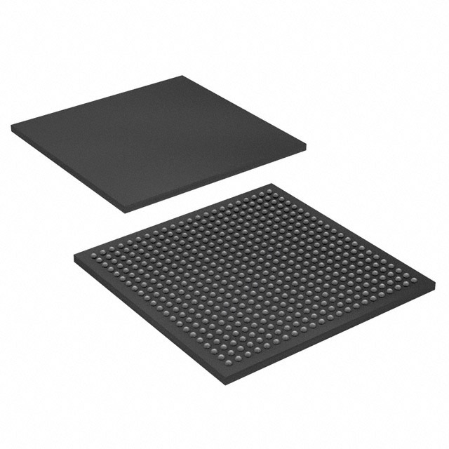
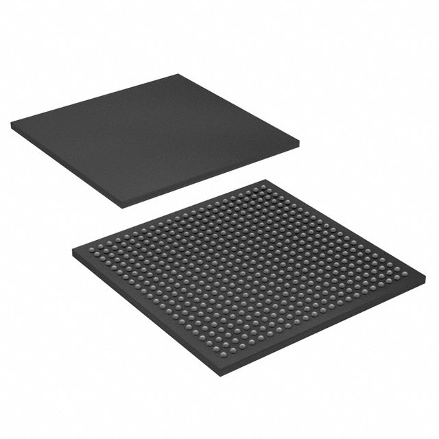
The EP2S60F484C5 is a Stratix II family Field Programmable Gate Array (FPGA) device from Intel (Altera) provided in a 484‑ball BGA package. It integrates a high logic density fabric with dedicated memory, DSP capabilities, and advanced clocking to support complex digital designs.
This device targets applications that require large on‑chip logic and memory resources, extensive I/O, and flexible clocking and configuration options as documented in the Stratix II device handbook.
Key Features
- Logic Capacity — 60,440 logic elements supporting complex combinational and sequential logic implementations; organized into 3,022 LABs (logic array blocks).
- Embedded Memory — Approximately 2.54 Mbits of on‑chip RAM (2,544,192 total RAM bits) for buffering, state storage, and memory‑based functions.
- I/O Resources — 334 general I/O pins to support multiple external interfaces and parallel connectivity requirements.
- Clocking and PLLs — Stratix II family clocking architecture including enhanced and fast PLLs and hierarchical global clock networks as detailed in the device handbook.
- DSP and Interface Support — On‑chip digital signal processing blocks and high‑speed I/O features referenced in the Stratix II documentation for signal processing and external memory interfacing.
- Configuration & Test — IEEE Std. 1149.1 JTAG boundary‑scan support and embedded logic analysis features (SignalTap II) described in the device handbook for debug and programming.
- Power Supply — Core voltage supply range of 1.15 V to 1.25 V for device operation.
- Package & Mounting — 484‑BBGA package (supplier device package: 484‑FBGA, 23×23); surface‑mount device suitable for compact PCB designs.
- Operating Conditions — Commercial grade operation from 0°C to 85°C.
- RoHS Compliance — Device is RoHS compliant.
Typical Applications
- Digital Signal Processing — Implement high‑throughput DSP pipelines using the Stratix II DSP blocks combined with large logic capacity and on‑chip RAM.
- High‑Speed Interface Control — Manage external memory interfaces and fast serial/parallel links using the device's high‑speed I/O capabilities and dedicated interface circuitry.
- System Clocking and Timing — Create multi‑clock systems and precision timing networks leveraging enhanced and fast PLLs and global clocking resources.
- Embedded System Integration — Consolidate control, glue logic, and peripheral interfaces in a single FPGA using abundant logic elements and I/O resources.
Unique Advantages
- High integration of logic and memory: 60,440 logic elements and approximately 2.54 Mbits of embedded memory reduce external component count and simplify board design.
- Extensive I/O capacity: 334 I/O pins enable broad external connectivity for parallel buses, peripheral interfaces, and mixed I/O standards described in the Stratix II handbook.
- Advanced clocking infrastructure: Enhanced and fast PLLs plus hierarchical clock networks provide flexible, low‑skew timing for multi‑domain designs.
- Built‑in test and configuration support: IEEE 1149.1 JTAG boundary‑scan and SignalTap II debug facilities streamline bring‑up and in‑system verification.
- Commercial operating range: Rated for 0°C to 85°C operation, suitable for a wide range of commercial electronics applications.
- Compact BGA footprint: 484‑ball FBGA (23×23) package and surface‑mount mounting help minimize PCB area while supporting high pin count.
Why Choose EP2S60F484C5?
The EP2S60F484C5 delivers a combination of high logic density, substantial embedded RAM, and broad I/O resources within the Stratix II architecture. Its documented features—DSP blocks, advanced PLLs, and on‑chip memory—support complex signal processing, interface bridging, and multi‑clock systems while reducing external component needs.
This device is well suited for design teams that need a commercially graded FPGA with comprehensive configuration and test support as detailed in the Stratix II device handbook. Selecting EP2S60F484C5 provides scalability and documented architectural resources from the Stratix II family to support development and deployment across demanding commercial applications.
Request a quote or submit an inquiry to receive pricing and availability for EP2S60F484C5 and to discuss how this Stratix II FPGA can fit your next design.





















Date Founded: 1968
Headquarters: Santa Clara, California, USA
Employees: 130,000+
Revenue: $54.23 Billion
Certifications and Memberships: ISO9001:2015, ISO14001:2015, ISO17025:2017, ISO27001:2022, ISO45001:2018, ISO50001:2018


