
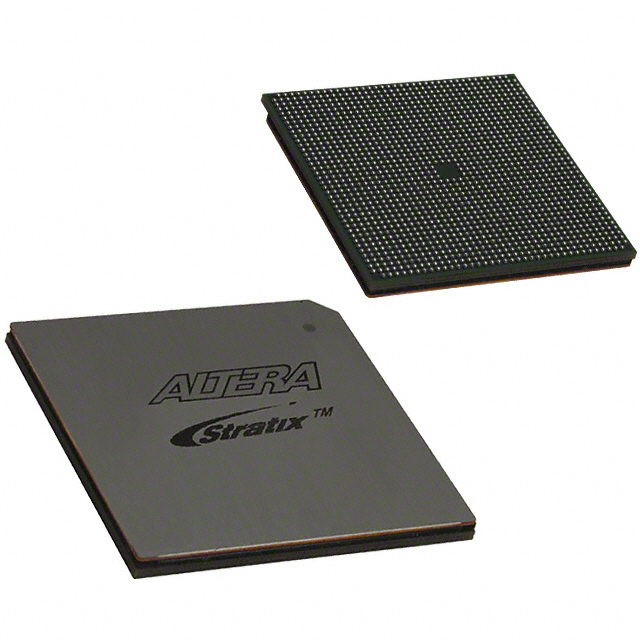
EP2SGX130GF1508C3
| Part Description |
Stratix® II GX Field Programmable Gate Array (FPGA) IC 734 6747840 132540 1508-BBGA, FCBGA |
|---|---|
| Quantity | 504 Available (as of June 14, 2026) |

| Product Category | Field Programmable Gate Array (FPGA) |
|---|---|
| Manufacturer | Intel |
| Manufacturing Status | Obsolete |
| Manufacturer Standard Lead Time | Contact Us |
| Datasheet |
Specifications & Environmental
| Device Package | 1508-FBGA, FC (40x40) | Grade | Commercial | Operating Temperature | 0°C – 85°C | ||
|---|---|---|---|---|---|---|---|
| Package / Case | 1508-BBGA, FCBGA | Number of I/O | 734 | Voltage | 1.15 V - 1.25 V | ||
| Mounting Method | Surface Mount | RoHS Compliance | RoHS non-compliant | REACH Compliance | REACH Unaffected | ||
| Moisture Sensitivity Level | 3 (168 Hours) | Number of LABs/CLBs | 6627 | Number of Logic Elements/Cells | 132540 | ||
| Number of Gates | N/A | ECCN | 3A001A7A | HTS Code | 8542.39.0001 | ||
| Qualification | N/A | Total RAM Bits | 6747840 |
Overview of EP2SGX130GF1508C3 – Stratix® II GX Field Programmable Gate Array (FPGA), 1508-BBGA
The EP2SGX130GF1508C3 is a Stratix® II GX FPGA IC from Intel, delivered in a 1508-BBGA (FCBGA) package for surface-mount applications. It combines a high-capacity logic array with substantial embedded memory and a large I/O count, targeting designs that require dense logic, on-chip RAM, and broad interfacing capability.
As a member of the Stratix II GX family, the device aligns with applications that demand scalable logic performance and advanced transceiver-enabled communications, while offering a commercial-grade operating range and RoHS compliance.
Key Features
- Logic Capacity Provides 132,540 logic elements suitable for complex programmable logic implementations and large-scale FPGA designs.
- Embedded Memory Approximately 6.75 Mbits of on-chip RAM to implement FIFOs, dual-port memories, and buffering without external memory for many functions.
- I/O Density 734 I/O pins to support high-pin-count interfaces and multi-channel external connectivity in demanding I/O architectures.
- Stratix II GX Family Transceiver Features Family-level transceiver capabilities include high-speed serial channels with clock-data recovery, adaptive equalization, programmable pre-emphasis and VOD, and dynamic reconfiguration to support multiple serial protocols and data rates.
- Clocking and DSP Resources Family features include multiple global and regional clock networks, enhanced PLLs for flexible clocking, and high-speed DSP blocks for multiplier and FIR implementations.
- Package & Mounting 1508‑BBGA (1508‑FBGA, FC, 40×40) surface-mount package appropriate for dense board layouts and automated assembly processes.
- Power Supply Operates from a core supply in the 1.15 V to 1.25 V range for compatibility with modern low-voltage systems.
- Operating Range & Compliance Commercial-grade operating temperature from 0 °C to 85 °C and RoHS-compliant manufacturing.
Typical Applications
- High-speed communications Implement protocol bridging, line cards, and chip-to-chip serialization using the Stratix II GX family’s high-speed transceiver capabilities.
- Backplane and switching systems Large logic capacity and abundant I/O make the device suitable for switch fabrics and backplane interface logic.
- Memory interface and buffering Embedded RAM and DSP resources enable on-chip buffering, FIFO management, and data path processing for external memory subsystems.
- Signal processing DSP blocks and substantial logic resources support FPGA-based signal processing functions such as filtering and accumulation.
Unique Advantages
- High logic density: 132,540 logic elements provide the room needed to implement complex state machines, datapaths, and control logic without partitioning across multiple devices.
- Significant on-chip memory: Approximately 6.75 Mbits of embedded RAM reduces dependence on external memory for many buffering and FIFO requirements.
- Extensive I/O capability: 734 I/Os enable integration of multiple parallel interfaces and high-pin-count system connections from a single FPGA package.
- Family-level high-speed serial support: Stratix II GX transceiver features (CDR, programmable VOD and pre-emphasis, adaptive equalization) support robust serial links and protocol flexibility.
- Flexible clocking and DSP support: On-device PLLs, global/regional clock networks, and DSP blocks facilitate complex timing architectures and high-performance math operations.
- Commercial-grade & RoHS-compliant: Designed for standard commercial-temperature deployments with environmental compliance for streamlined procurement.
Why Choose EP2SGX130GF1508C3?
The EP2SGX130GF1508C3 delivers a balance of high logic capacity, sizeable embedded memory, and very large I/O count in a compact 1508‑BBGA package. As part of the Stratix II GX family, it provides a platform that supports sophisticated clocking, DSP acceleration, and family-level transceiver technologies for high-speed serial communications.
This combination makes the device well suited for designers building advanced communications, backplane interface, and data-processing systems that require scalable logic resources, on-chip memory for buffering, and the flexibility to implement multiple high-pin-count interfaces within a single FPGA.
Request a quote or submit an inquiry to evaluate EP2SGX130GF1508C3 for your design and obtain pricing and availability information.


Date Founded: 1968
Headquarters: Santa Clara, California, USA
Employees: 130,000+
Revenue: $54.23 Billion
Certifications and Memberships: ISO9001:2015, ISO14001:2015, ISO17025:2017, ISO27001:2022, ISO45001:2018, ISO50001:2018


