
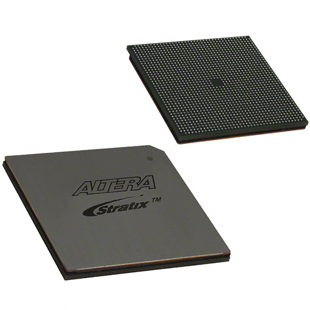
EP2SGX130GF1508C3N
| Part Description |
Stratix® II GX Field Programmable Gate Array (FPGA) IC 734 6747840 132540 1508-BBGA, FCBGA |
|---|---|
| Quantity | 1,586 Available (as of June 14, 2026) |

| Product Category | Field Programmable Gate Array (FPGA) |
|---|---|
| Manufacturer | Intel |
| Manufacturing Status | Obsolete |
| Manufacturer Standard Lead Time | Contact Us |
| Datasheet |
Specifications & Environmental
| Device Package | 1508-FBGA, FC (40x40) | Grade | Commercial | Operating Temperature | 0°C – 85°C | ||
|---|---|---|---|---|---|---|---|
| Package / Case | 1508-BBGA, FCBGA | Number of I/O | 734 | Voltage | 1.15 V - 1.25 V | ||
| Mounting Method | Surface Mount | RoHS Compliance | RoHS Compliant | REACH Compliance | REACH Unaffected | ||
| Moisture Sensitivity Level | 3 (168 Hours) | Number of LABs/CLBs | 6627 | Number of Logic Elements/Cells | 132540 | ||
| Number of Gates | N/A | ECCN | 3A001A7A | HTS Code | 8542.39.0001 | ||
| Qualification | N/A | Total RAM Bits | 6747840 |
Overview of EP2SGX130GF1508C3N – Stratix® II GX FPGA, 1508-BBGA
The EP2SGX130GF1508C3N is a Stratix® II GX field programmable gate array (FPGA) device combining a high-performance logic array with the Stratix II GX family’s high-speed serial transceiver architecture. It delivers a dense logic fabric and substantial on-chip memory together with a large I/O count and an FCBGA 1508 package targeted at commercial embedded and communications designs.
Typical use cases include high-speed backplane interfaces, chip-to-chip bridging, and communications protocol implementation where integrated transceivers, DSP resources and memory bandwidth support complex, high-throughput designs.
Key Features
- Logic Capacity — 132,540 logic elements for implementating complex digital functions and large-scale custom logic.
- Embedded Memory — Approximately 6.75 Mbits of on-chip RAM to support FIFOs, buffers and packet/frame buffering.
- I/O Density — 734 user I/O pins to support wide parallel interfaces and multi-channel connectivity.
- Stratix II GX Family Transceivers — Family-level support for high-speed serial transceivers with data rates up to 6.375 Gbps and multi-channel configurations (family devices available with 4 to 20 channels), enabling high-bandwidth serial links.
- DSP and Clocking — Stratix II GX family features include high-speed DSP blocks and up to four enhanced PLLs for advanced clock management and real-time PLL reconfiguration (family-level capability documented in the device handbook).
- Packaging & Mounting — 1508-BBGA (FCBGA) package; supplier device package listed as 1508-FBGA, FC (40×40). Surface-mount mounting type.
- Power & Temperature — Core supply range 1.15 V to 1.25 V; commercial operating temperature range 0 °C to 85 °C.
- Compliance — RoHS compliant.
Typical Applications
- High‑speed Communications — Implements protocol bridging and line-rate serial interfaces using the family’s high-speed transceiver support and large I/O count.
- Backplane & Switch Fabric — Suitable for high-throughput backplane interfaces where dense logic and on-chip memory enable packet buffering and routing functions.
- Chip‑to‑Chip Interconnect — Facilitates high-bandwidth chip-to-chip links leveraging serial transceivers and abundant user I/O.
- Signal Processing — On-chip DSP resources and sizable embedded RAM support FIR filters, multiply-accumulate and other streaming DSP tasks (family features described in the device handbook).
Unique Advantages
- High Logic Density: 132,540 logic elements let you implement complex control and datapath logic without external glue logic.
- Substantial On‑Chip Memory: Approximately 6.75 Mbits of embedded RAM reduces external memory dependency for buffering and FIFOs.
- High I/O Count: 734 I/Os provide flexibility for parallel buses, multiple interfaces and board-level routing options.
- Integrated High‑Speed Serial Capability: Stratix II GX family transceivers (up to 6.375 Gbps) enable direct implementation of high-bandwidth serial links.
- Commercial Temperature and Standard Supply: Operates across a common commercial range (0 °C to 85 °C) with a defined core voltage window (1.15–1.25 V) for predictable power design.
- RoHS Compliant: Supports regulatory requirements for lead‑free manufacturing.
Why Choose EP2SGX130GF1508C3N?
The EP2SGX130GF1508C3N positions itself as a high-capacity Stratix II GX FPGA option for designs that require a combination of large logic resources, substantial embedded memory and a very high I/O count in a 1508‑ball FCBGA package. Its family-level transceiver and DSP capabilities make it suitable for communications, backplane and signal-processing applications where integrated bandwidth and on-chip resources reduce system complexity.
For engineering teams seeking scalability and a proven FPGA architecture, this device provides measurable resources and the documented Stratix II GX family features to support complex, high-throughput designs with commercial-grade temperature and RoHS compliance.
Request a quote or submit an inquiry to receive pricing, availability and ordering information for EP2SGX130GF1508C3N.


Date Founded: 1968
Headquarters: Santa Clara, California, USA
Employees: 130,000+
Revenue: $54.23 Billion
Certifications and Memberships: ISO9001:2015, ISO14001:2015, ISO17025:2017, ISO27001:2022, ISO45001:2018, ISO50001:2018


