
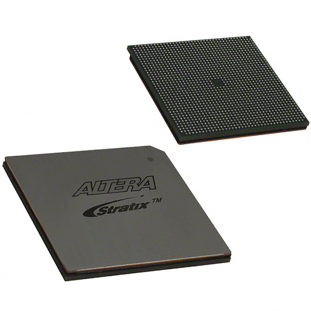
EP2SGX130GF1508I4
| Part Description |
Stratix® II GX Field Programmable Gate Array (FPGA) IC 734 6747840 132540 1508-BBGA, FCBGA |
|---|---|
| Quantity | 1,089 Available (as of June 16, 2026) |

| Product Category | Field Programmable Gate Array (FPGA) |
|---|---|
| Manufacturer | Intel |
| Manufacturing Status | Obsolete |
| Manufacturer Standard Lead Time | Contact Us |
| Datasheet |
Specifications & Environmental
| Device Package | 1508-FBGA, FC (40x40) | Grade | Industrial | Operating Temperature | -40°C – 100°C | ||
|---|---|---|---|---|---|---|---|
| Package / Case | 1508-BBGA, FCBGA | Number of I/O | 734 | Voltage | 1.15 V - 1.25 V | ||
| Mounting Method | Surface Mount | RoHS Compliance | RoHS non-compliant | REACH Compliance | REACH Unaffected | ||
| Moisture Sensitivity Level | 3 (168 Hours) | Number of LABs/CLBs | 6627 | Number of Logic Elements/Cells | 132540 | ||
| Number of Gates | N/A | ECCN | 3A001A7A | HTS Code | 8542.39.0001 | ||
| Qualification | N/A | Total RAM Bits | 6747840 |
Overview of EP2SGX130GF1508I4 – Stratix® II GX FPGA, 132,540 logic elements, 1508‑BBGA
The EP2SGX130GF1508I4 is a Stratix II GX family field programmable gate array (FPGA) offered in a 1508‑ball BGA package for surface‑mount applications. It provides a scalable logic array, on‑chip embedded memory, and a high I/O count suitable for industrial designs requiring dense logic and flexible I/O.
Targeted at high‑performance communications and system‑level applications, this device combines a large logic capacity with multi‑gigabit transceiver technology (described in the Stratix II GX device handbook) to support high‑speed interfaces, memory controllers, and complex protocol bridging while operating across an industrial temperature range.
Key Features
- Logic Capacity — 6,627 logic array blocks with approximately 132,540 logic elements to implement complex RTL, state machines, and custom datapaths.
- Embedded Memory — Approximately 6.75 Mbits of on‑chip RAM for FIFOs, buffers, and packet or frame storage.
- I/O Density — 734 user I/O pins to support wide parallel interfaces, multiple memory buses, and high pin‑count system interconnects.
- High‑Speed Transceiver Technology (Stratix II GX family) — Family device handbook describes high‑speed serial transceivers capable of up to 6.375 Gbps and devices with 4–20 channels for multi‑Gbps links and protocol bridging.
- DSP and Clocking Resources — Family features include dedicated high‑speed DSP blocks and up to four enhanced PLLs for high‑performance multiply/accumulate operations and advanced clock management (as described in the Stratix II GX documentation).
- Power Supply — Core supply range from 1.15 V to 1.25 V for the logic array.
- Package & Mounting — 1508‑BBGA / FCBGA package (supplier package: 1508‑FBGA, FC 40×40) in a surface‑mount format for compact board integration.
- Industrial Temperature Grade — Rated for operation from −40 °C to 100 °C, meeting industrial environmental requirements.
- Standards & Support (Series) — The Stratix II GX family documentation details support for multiple I/O standards, advanced memory interfaces, and design security features such as bitstream encryption and remote configuration.
- RoHS Compliant — Device complies with RoHS requirements for lead‑free assembly processes.
Typical Applications
- High‑speed communications — Implement multi‑Gbps link aggregation, protocol bridging, and serial backplane interfaces using the Stratix II GX transceiver capabilities.
- Network & Telecom infrastructure — Use the large logic and memory resources for packet buffering, traffic management, and protocol conversion in industrial network equipment.
- High‑performance system controllers — Leverage dense logic and abundant I/O for complex control, bridging multiple parallel and serial buses in embedded systems.
- Memory interface and buffering — Implement controllers and high‑throughput FIFOs for DDR/QDR memory front ends and external memory subsystems.
Unique Advantages
- High logic density: Approximately 132,540 logic elements enable implementation of large, complex designs without external glue logic.
- Substantial embedded memory: About 6.75 Mbits of on‑chip RAM reduces the need for external buffering and simplifies board-level memory design.
- Extensive I/O count: 734 I/O pins allow simultaneous connection to multiple peripherals, wide data buses, and parallel interfaces.
- Industrial robustness: −40 °C to 100 °C operating range supports deployment in demanding environments.
- Compact board integration: 1508‑BBGA surface‑mount package provides a high pin‑count solution in a compact footprint for dense system boards.
- Vendor family features: Access to the Stratix II GX family’s transceiver, DSP, and clocking resources described in the device handbook for advanced interface and signal processing requirements.
Why Choose EP2SGX130GF1508I4?
The EP2SGX130GF1508I4 positions itself as a high‑capacity, industrial‑grade FPGA option within the Stratix II GX family, combining a large logic fabric, significant embedded memory, and a very high I/O count in a compact BGA package. It is well suited to systems that demand dense logic implementation, robust operating temperature margins, and support for high‑speed serial and parallel interfaces as documented in the Stratix II GX device handbook.
Design teams targeting communications, network infrastructure, or high‑performance embedded controllers will find the combination of logic resources, on‑chip RAM, and family‑level transceiver and DSP capabilities advantageous for reducing external components, simplifying board design, and enabling flexible reprogrammability over the product lifecycle.
Request a quote or submit an inquiry to receive pricing, availability, and lead‑time information for EP2SGX130GF1508I4.


Date Founded: 1968
Headquarters: Santa Clara, California, USA
Employees: 130,000+
Revenue: $54.23 Billion
Certifications and Memberships: ISO9001:2015, ISO14001:2015, ISO17025:2017, ISO27001:2022, ISO45001:2018, ISO50001:2018


