
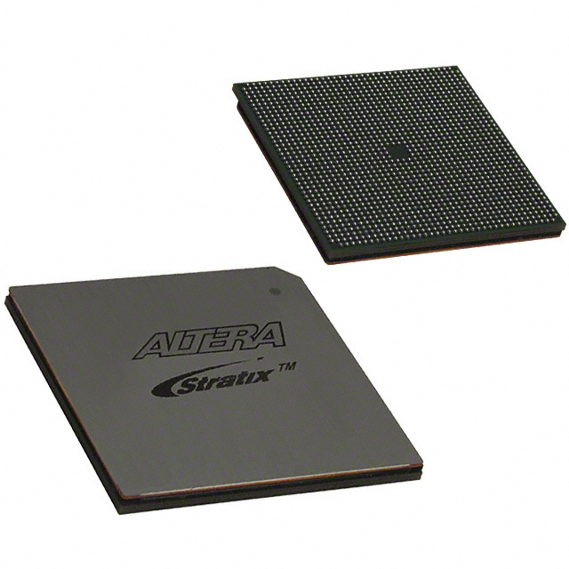
EP2SGX130GF1508C4N
| Part Description |
Stratix® II GX Field Programmable Gate Array (FPGA) IC 734 6747840 132540 1508-BBGA, FCBGA |
|---|---|
| Quantity | 146 Available (as of June 15, 2026) |

| Product Category | Field Programmable Gate Array (FPGA) |
|---|---|
| Manufacturer | Intel |
| Manufacturing Status | Obsolete |
| Manufacturer Standard Lead Time | Contact Us |
| Datasheet |
Specifications & Environmental
| Device Package | 1508-FBGA, FC (40x40) | Grade | Commercial | Operating Temperature | 0°C – 85°C | ||
|---|---|---|---|---|---|---|---|
| Package / Case | 1508-BBGA, FCBGA | Number of I/O | 734 | Voltage | 1.15 V - 1.25 V | ||
| Mounting Method | Surface Mount | RoHS Compliance | RoHS Compliant | REACH Compliance | REACH Unaffected | ||
| Moisture Sensitivity Level | 3 (168 Hours) | Number of LABs/CLBs | 6627 | Number of Logic Elements/Cells | 132540 | ||
| Number of Gates | N/A | ECCN | 3A001A7A | HTS Code | 8542.39.0001 | ||
| Qualification | N/A | Total RAM Bits | 6747840 |
Overview of EP2SGX130GF1508C4N – Stratix® II GX FPGA, 132,540 logic elements, 1508-BBGA
The EP2SGX130GF1508C4N is a Stratix® II GX field programmable gate array (FPGA) from Intel, designed for high-density logic and embedded memory integration in commercial-grade systems. It combines a large logic array with on-chip RAM and a family-level architecture that includes high-speed serial transceiver capabilities.
Typical use cases include high-speed backplane interfaces, chip-to-chip bridging, and communications protocol applications where substantial logic resources, embedded memory, and robust I/O counts are required. The device is supplied in a 1508-ball FCBGA surface-mount package and operates within a 1.15 V–1.25 V supply range and a 0 °C to 85 °C commercial temperature window.
Key Features
- High Logic Density Provides 132,540 logic elements for complex digital designs and large-scale integration.
- Embedded Memory Includes approximately 6.75 Mbits of on-chip RAM to implement arrays, FIFOs, and dual-port memory structures.
- I/O Capacity Up to 734 I/O pins support extensive external interfacing for parallel buses, memory interfaces, and peripheral connectivity.
- Stratix II GX Family Transceiver Support The Stratix II GX family supports high-speed serial transceivers with channel data rates from 600 Mbps to 6.375 Gbps and family features for dynamic reconfiguration, adaptive equalization, and protocol support.
- Clocking and DSP Resources Family-level architecture provides multiple global and regional clock networks and high-speed DSP blocks (for multiply and MAC operations) suitable for signal processing tasks.
- Power and Supply Device operates from a core supply range of 1.15 V to 1.25 V, enabling predictable core power budgeting.
- Package and Mounting Delivered in a 1508-BBGA (FCBGA) surface-mount package (40 mm × 40 mm supplier outline) for high-density board layouts.
- Commercial Grade Specified for 0 °C to 85 °C operation and RoHS compliant for standard commercial applications.
Typical Applications
- High-Speed Backplane Interfaces Leverages the Stratix II GX family transceiver capabilities and high logic density to implement packet switching, protocol bridging, and backplane SERDES interfaces.
- Chip-to-Chip and Protocol Bridging Large logic and embedded memory support complex protocol translation and data buffering between chips or subsystems.
- Communications Systems Suitable for network and telecom equipment designs that require substantial logic resources and family-level support for standards such as PCI Express and Ethernet.
- Memory and Buffering Controllers On-chip RAM and I/O count support memory controller implementations and high-bandwidth buffering for external DDR/QDR interfaces.
Unique Advantages
- High-density programmable fabric: 132,540 logic elements enable integration of large, complex designs onto a single device, reducing board-level component count.
- Embedded on-chip memory: Approximately 6.75 Mbits of RAM provides local storage for FIFOs, buffers, and dual-port memory without external components.
- Rich I/O footprint: 734 I/O connections give designers flexibility for wide parallel interfaces, multi-channel connections, and extensive peripheral support.
- Family-level high-speed serial support: Stratix II GX transceiver features (600 Mbps–6.375 Gbps) enable high-throughput serial links and protocol adaptability for communications designs.
- Commercial temperature and RoHS compliant: Rated for 0 °C to 85 °C operation and RoHS compliance for standard commercial deployments.
- Surface-mount, high-density package: 1508-BBGA (FCBGA) package supports compact PCB layouts and high I/O routing density.
Why Choose EP2SGX130GF1508C4N?
The EP2SGX130GF1508C4N positions itself as a high-density Stratix II GX solution for commercial designs that require large programmable logic capacity, embedded memory, and extensive I/O. Its family-level transceiver capabilities and DSP/clocking architecture make it well suited to demanding communications, interface, and protocol-bridging applications.
Designed for engineers and system designers needing scalable performance with Intel’s Stratix II GX architecture, this device offers integration that can reduce BOM complexity while providing the on-chip resources to handle memory buffering, high-throughput I/O, and complex logic functions.
Request a quote or submit an inquiry to learn about availability, pricing, and lead times for the EP2SGX130GF1508C4N.


Date Founded: 1968
Headquarters: Santa Clara, California, USA
Employees: 130,000+
Revenue: $54.23 Billion
Certifications and Memberships: ISO9001:2015, ISO14001:2015, ISO17025:2017, ISO27001:2022, ISO45001:2018, ISO50001:2018


