
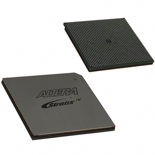
EP2SGX130GF1508C5N
| Part Description |
Stratix® II GX Field Programmable Gate Array (FPGA) IC 734 6747840 132540 1508-BBGA, FCBGA |
|---|---|
| Quantity | 606 Available (as of June 15, 2026) |
| Product Category | Field Programmable Gate Array (FPGA) |
|---|---|
| Manufacturer | Intel |
| Manufacturing Status | Obsolete |
| Manufacturer Standard Lead Time | Contact Us |
| Datasheet |
Specifications & Environmental
| Device Package | 1508-FBGA, FC (40x40) | Grade | Commercial | Operating Temperature | 0°C – 85°C | ||
|---|---|---|---|---|---|---|---|
| Package / Case | 1508-BBGA, FCBGA | Number of I/O | 734 | Voltage | 1.15 V - 1.25 V | ||
| Mounting Method | Surface Mount | RoHS Compliance | RoHS Compliant | REACH Compliance | REACH Unaffected | ||
| Moisture Sensitivity Level | 3 (168 Hours) | Number of LABs/CLBs | 6627 | Number of Logic Elements/Cells | 132540 | ||
| Number of Gates | N/A | ECCN | 3A001A7A | HTS Code | 8542.39.0001 | ||
| Qualification | N/A | Total RAM Bits | 6747840 |
Overview of EP2SGX130GF1508C5N – Stratix II GX FPGA, 1508-BBGA FCBGA
The EP2SGX130GF1508C5N is a Stratix® II GX family Field Programmable Gate Array (FPGA) in a 1508-BBGA FCBGA package. It pairs a scalable, high-performance logic array with the Stratix II GX family’s high-speed serial transceiver architecture to address demanding communications and system-integration applications.
Targeted at high-speed backplane, chip-to-chip and protocol-bridging designs, this device delivers extensive logic and I/O resources alongside family-level transceiver and clocking capabilities for designs that require flexible integration and high data throughput.
Key Features
- Logic Capacity 132,540 logic elements for complex digital implementation and system integration tasks.
- Embedded Memory Approximately 6.75 Mbits of on-chip RAM to implement FIFOs, buffers, and embedded data storage.
- I/O Density 734 I/O pins, supporting a variety of interface requirements and high pin-count system designs.
- High-Speed Transceiver Family Features Stratix II GX family transceivers support 600 Mbps to 6.375 Gbps per channel, dynamic reconfiguration, adaptive equalization, and programmable transmitter pre-emphasis for robust high-speed links.
- Clocking and DSP Family features include up to four enhanced PLLs and high-speed DSP blocks for multipliers and MAC functions, enabling accelerated signal processing and efficient clock management.
- Memory & External Interface Support Family-level support for high-speed external memory standards (QDR, DDR, DDR2) and a broad range of single-ended and differential I/O standards.
- Power and Supply Core voltage supply range from 1.15 V to 1.25 V to match system power architectures.
- Package & Mounting 1508-BBGA, FCBGA package (supplier device package: 1508-FBGA, FC 40×40); surface-mount construction for compact PCB integration.
- Operating Range & Compliance Commercial-grade operating temperature 0 °C to 85 °C and RoHS compliant.
Typical Applications
- High-speed Backplane Interfaces Use the Stratix II GX family transceivers and dense logic to implement high-throughput backplane protocols and multi-lane links.
- Chip-to-Chip Communications Leverage high I/O count and serial transceiver features for low-latency, high-bandwidth board-level interconnects.
- Protocol Bridging and Aggregation Combine abundant logic elements and embedded memory to translate, aggregate, or bridge between serial and parallel protocols in communications equipment.
- High-performance Signal Processing Utilize on-device DSP blocks and embedded RAM for FIR filters, MAC operations, and streaming data manipulation.
Unique Advantages
- Large Logic Fabric: 132,540 logic elements support complex, system-level designs without immediate need for external glue logic.
- Substantial Embedded Memory: Approximately 6.75 Mbits of on-chip RAM enables efficient buffering and FIFO implementations directly on the FPGA.
- Family Transceiver Capabilities: Stratix II GX transceiver technology delivers multi-gigabit serial links with adaptive equalization and programmable output conditioning to improve link integrity.
- Rich I/O Mix: 734 I/O pins provide flexibility to connect many peripherals, memory interfaces, and high-speed interfaces on a single device.
- Comprehensive Clocking and DSP Support: Enhanced PLLs and dedicated DSP blocks enable advanced timing architectures and signal-processing workloads within the FPGA fabric.
- Commercial-Grade and RoHS Compliant: Designed for commercial temperature ranges and compliant with RoHS requirements for broader deployment.
Why Choose EP2SGX130GF1508C5N?
The EP2SGX130GF1508C5N positions itself as a high-capacity Stratix II GX FPGA suitable for designs that need substantial logic, abundant embedded memory, and high I/O density combined with the family’s proven high-speed transceiver features. Its mix of on-chip resources and platform-level transceiver capabilities make it appropriate for communications, protocol conversion, and high-performance signal-processing applications.
Backed by Stratix II GX family documentation and design resources, this device offers scalable implementation options for teams developing systems requiring robust data throughput and flexible interface support, with long-term viability for projects operating within commercial temperature ranges.
Request a quote or submit a purchasing inquiry to get pricing, availability, and lead-time information for EP2SGX130GF1508C5N.


Date Founded: 1968
Headquarters: Santa Clara, California, USA
Employees: 130,000+
Revenue: $54.23 Billion
Certifications and Memberships: ISO9001:2015, ISO14001:2015, ISO17025:2017, ISO27001:2022, ISO45001:2018, ISO50001:2018


