
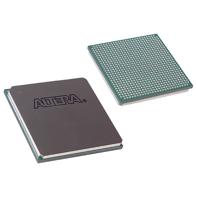
EP2SGX30CF780C3
| Part Description |
Stratix® II GX Field Programmable Gate Array (FPGA) IC 361 1369728 33880 780-BBGA |
|---|---|
| Quantity | 544 Available (as of June 15, 2026) |

| Product Category | Field Programmable Gate Array (FPGA) |
|---|---|
| Manufacturer | Intel |
| Manufacturing Status | Obsolete |
| Manufacturer Standard Lead Time | Contact Us |
| Datasheet |
Specifications & Environmental
| Device Package | 780-FBGA (29x29) | Grade | Commercial | Operating Temperature | 0°C – 85°C | ||
|---|---|---|---|---|---|---|---|
| Package / Case | 780-BBGA | Number of I/O | 361 | Voltage | 1.15 V - 1.25 V | ||
| Mounting Method | Surface Mount | RoHS Compliance | RoHS non-compliant | REACH Compliance | REACH Unaffected | ||
| Moisture Sensitivity Level | 3 (168 Hours) | Number of LABs/CLBs | 1694 | Number of Logic Elements/Cells | 33880 | ||
| Number of Gates | N/A | ECCN | 3A991D | HTS Code | 8542.39.0001 | ||
| Qualification | N/A | Total RAM Bits | 1369728 |
Overview of EP2SGX30CF780C3 – Stratix® II GX FPGA, 33,880 logic elements
The EP2SGX30CF780C3 is an Intel Stratix® II GX Field Programmable Gate Array (FPGA) in a 780-ball BGA package intended for commercial applications. It delivers a high-density logic array and substantial embedded memory, built on the Stratix II GX architecture described in the device datasheet.
Designed for high-performance digital designs, the device is suitable for applications that benefit from scalable logic resources, on-chip memory, and the Stratix II GX family’s high-speed serial capabilities as described in the datasheet.
Key Features
- Logic Density Approximately 33,880 logic elements to implement complex digital functions and custom logic.
- Embedded Memory Approximately 1.37 Mbits of on-chip RAM for FIFOs, buffers, and application memory needs.
- I/O Resources 361 general I/O pins to support a wide variety of external interfaces and board-level connectivity.
- Stratix II GX Architecture Built on the Stratix II GX device family which includes high-speed serial transceiver technology and advanced architecture elements described in the datasheet.
- Low-Voltage Core Core voltage supply range of 1.15 V to 1.25 V to match system power rail requirements.
- Package & Mounting 780-ball BGA (780-BBGA) with supplier device package specified as 780-FBGA (29×29); surface-mount package suitable for compact board layouts.
- Operating Range Commercial grade operation from 0 °C to 85 °C for typical commercial environments.
- Standards & Compliance RoHS compliant, supporting regulatory and environmental requirements for lead-free assembly.
- Family-Level High-Speed Features Stratix II GX devices include high-speed serial transceivers with data rates up to 6.375 Gbps and advanced transceiver features as described in the datasheet.
Typical Applications
- High-speed communications equipment Leverages the Stratix II GX family’s serial transceiver capabilities and on-chip memory for protocol bridging and packet processing.
- Backplane and board-to-board interfaces Suitable for high-speed backplane interface designs that require significant logic density and numerous I/O.
- Chip-to-chip bridging Provides programmable logic and memory resources to implement custom interface logic and real-time data handling between chips.
- Custom accelerator and DSP functions On-chip memory and the Stratix II GX architecture support implementation of DSP blocks and custom processing pipelines described in the device family documentation.
Unique Advantages
- Substantial logic capacity: Approximately 33,880 logic elements enable implementation of complex state machines, protocol stacks, and custom accelerators on a single device.
- Significant embedded memory: Approximately 1.37 Mbits of on-chip RAM reduces external memory needs for many buffering and FIFO requirements.
- High I/O count: 361 I/O pins provide flexibility to interface with multiple peripherals and bus architectures without large external glue logic.
- Stratix II GX family capabilities: Family-level support for high-speed serial transceivers and advanced architecture features provides design flexibility for high-bandwidth links (as described in the datasheet).
- Compact, surface-mount package: 780-ball BGA (29×29) package supports dense board layouts while maintaining the device’s thermal and electrical characteristics.
- RoHS compliant and commercial grade: Meets lead-free assembly requirements and is specified for 0 °C to 85 °C commercial operation.
Why Choose EP2SGX30CF780C3?
The EP2SGX30CF780C3 combines substantial logic resources, meaningful on-chip memory, and extensive I/O in a Stratix II GX device package. It is well suited to designers who need programmable capacity for protocol handling, data buffering, and custom processing within commercial temperature environments and with low-voltage core requirements.
Choosing this part gives access to the Stratix II GX device family features documented in the datasheet, enabling designs that require programmable high-speed link support, integrated memory resources, and a compact BGA footprint for space-constrained boards.
Request a quote or submit an inquiry to receive pricing and availability for EP2SGX30CF780C3 and to discuss how this FPGA can fit your design requirements.


Date Founded: 1968
Headquarters: Santa Clara, California, USA
Employees: 130,000+
Revenue: $54.23 Billion
Certifications and Memberships: ISO9001:2015, ISO14001:2015, ISO17025:2017, ISO27001:2022, ISO45001:2018, ISO50001:2018


