
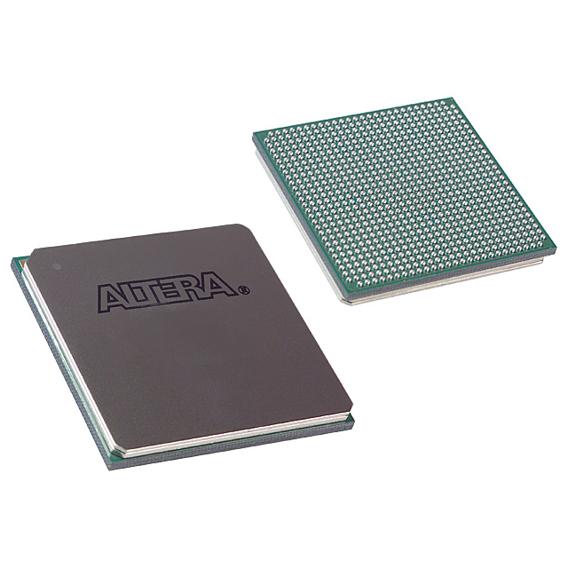
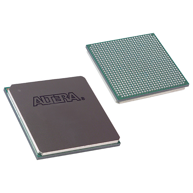
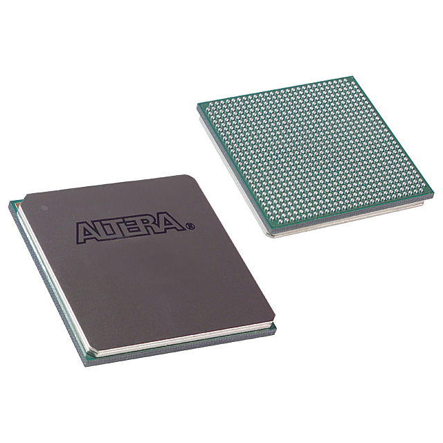
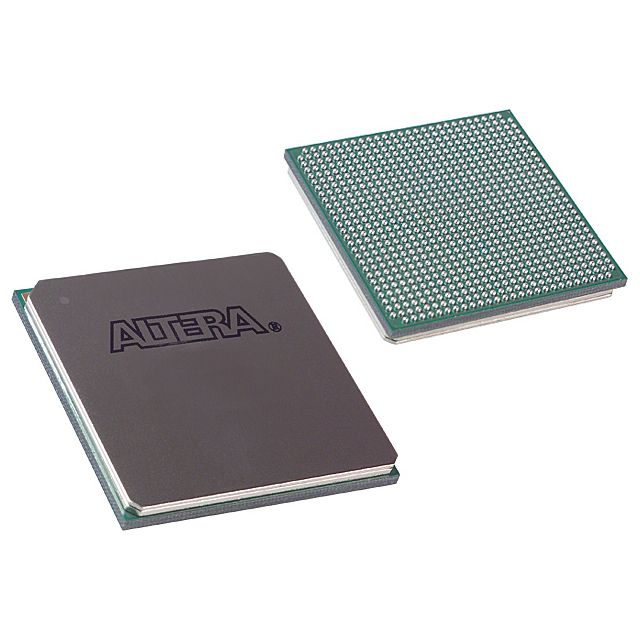
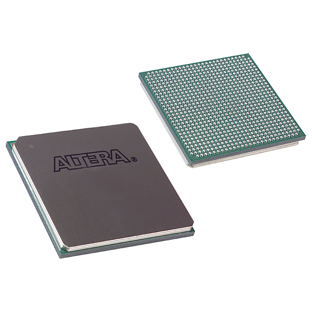
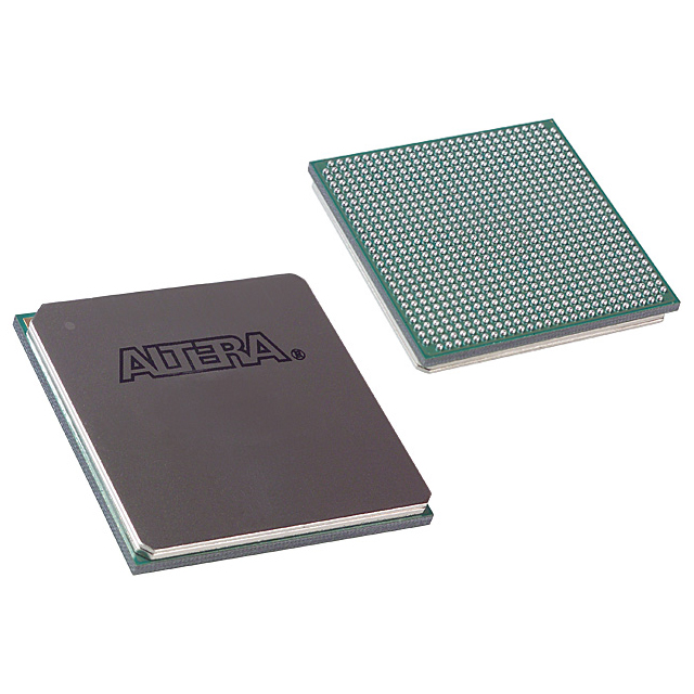
EP2SGX30CF780C5
| Part Description |
Stratix® II GX Field Programmable Gate Array (FPGA) IC 361 1369728 33880 780-BBGA |
|---|---|
| Quantity | 945 Available (as of October 7, 2026) |
| Product Category | Field Programmable Gate Array (FPGA) |
|---|---|
| Manufacturer | Intel |
| Manufacturing Status | Obsolete |
| Manufacturer Standard Lead Time | Contact Us |
| Datasheet |
Specifications & Environmental
| Device Package | 780-FBGA (29x29) | Grade | Commercial | Operating Temperature | 0°C – 85°C | ||
|---|---|---|---|---|---|---|---|
| Package / Case | 780-BBGA | Number of I/O | 361 | Voltage | 1.15 V - 1.25 V | ||
| Mounting Method | Surface Mount | RoHS Compliance | RoHS non-compliant | REACH Compliance | REACH Unaffected | ||
| Moisture Sensitivity Level | 3 (168 Hours) | Number of LABs/CLBs | 1694 | Number of Logic Elements/Cells | 33880 | ||
| Number of Gates | N/A | ECCN | 3A991D | HTS Code | 8542.39.0001 | ||
| Qualification | N/A | Total RAM Bits | 1369728 |
Overview of EP2SGX30CF780C5 – Stratix® II GX FPGA, 780‑BBGA
The EP2SGX30CF780C5 is a Stratix II GX field-programmable gate array (FPGA) in a 780‑ball BGA package. It provides a scalable, high-performance logic array with a low-voltage core and a rich set of I/O for demanding connectivity and protocol-bridging applications.
Built on the Stratix II GX family architecture, the device is targeted at high-speed backplane interfaces, chip-to-chip links and communication protocol bridging where integrated transceiver capability, on-chip memory and DSP resources speed development and deployment.
Key Features
- Logic Capacity — 33,880 logic elements (cells) to implement complex state machines, control logic and custom datapaths.
- Embedded Memory — Approximately 1.37 Mbits of on-chip RAM for FIFOs, buffering and fast local storage.
- I/O Density — 361 user I/O pins to support wide parallel interfaces and mixed single-ended/differential signaling.
- Family Transceiver Capabilities — Stratix II GX family devices include high-speed serial transceivers with full-duplex operation up to 6.375 Gbps and support for common serial protocols and dynamic reconfiguration (family-level capability described in the device datasheet).
- Clocking and DSP (Family) — Family architecture includes up to 16 global clock networks, regional clock resources, high-speed DSP blocks for multiply-accumulate functions and enhanced PLLs for flexible clock management (family-level features).
- Package & Mounting — 780‑BBGA (supplier package listed as 780‑FBGA, 29×29) in a surface-mount format for compact board integration.
- Power — Core supply range 1.15 V to 1.25 V to interface with modern low‑voltage systems.
- Commercial Temperature Grade — Rated for 0 °C to 85 °C operation; device grade: Commercial.
- RoHS Compliant — Meets lead‑free and hazardous‑substance requirements for environmental compliance.
Typical Applications
- High‑speed Backplane Interfaces — Implements complex bridging and packet handling for backplane fabrics using the family’s high-speed serial capabilities and large logic capacity.
- Chip‑to‑Chip Connectivity — Provides SERDES-based links and flexible I/O pin count to connect multiple devices across PCBs or within chassis.
- Communications Protocol Bridging — Ideal for translating or aggregating protocols where family transceiver features and on-chip memory simplify protocol handling and buffering.
- Signal Processing and DSP Tasks — On-chip RAM and family DSP resources support FIR filters, MAC operations and other real‑time data processing functions.
Unique Advantages
- Substantial Logic Density: 33,880 logic elements allow integration of large custom logic blocks and state machines, reducing external component count.
- Significant Embedded Memory: Approximately 1.37 Mbits of RAM enables deep buffering and efficient FIFO implementations close to the logic.
- High I/O Count in a Compact Package: 361 I/Os in a 780‑ball BGA (29×29) package support wide parallel buses and varied signaling options while maintaining a small PCB footprint.
- Low‑Voltage Core: 1.15–1.25 V core supply aligns with contemporary system power rails for efficient integration.
- Family Transceiver and IP Support: Stratix II GX family transceiver features and support for MegaCore/AMPP megafunctions (as described in the datasheet) streamline high-speed protocol implementation and accelerate development.
- Commercial Temperature Rating & RoHS Compliance: Clear operational range (0 °C to 85 °C) and environmental compliance simplify qualification for commercial products.
Why Choose EP2SGX30CF780C5?
The EP2SGX30CF780C5 combines a high-density logic fabric, substantial on-chip RAM and the Stratix II GX family’s advanced transceiver and clocking architecture to address demanding connectivity and processing tasks. Its package density and 361 I/Os make it suitable for systems that require compact, high‑function integration while operating within commercial temperature ranges.
This device is a practical choice for engineering teams designing high‑speed communications, protocol bridging and signal processing applications that benefit from integrated memory, DSP resources and family-level transceiver capabilities described in the Stratix II GX datasheet.
Request a quote or submit an inquiry to receive pricing and availability information for EP2SGX30CF780C5. Our team will respond with lead time and ordering details to help you move your design forward.





















Date Founded: 1968
Headquarters: Santa Clara, California, USA
Employees: 130,000+
Revenue: $54.23 Billion
Certifications and Memberships: ISO9001:2015, ISO14001:2015, ISO17025:2017, ISO27001:2022, ISO45001:2018, ISO50001:2018


