
EP2SGX30DF780C4N
| Part Description |
Stratix® II GX Field Programmable Gate Array (FPGA) IC 361 1369728 33880 780-BBGA |
|---|---|
| Quantity | 382 Available (as of June 15, 2026) |
| Product Category | Field Programmable Gate Array (FPGA) |
|---|---|
| Manufacturer | Intel |
| Manufacturing Status | Obsolete |
| Manufacturer Standard Lead Time | Contact Us |
| Datasheet |
Specifications & Environmental
| Device Package | 780-FBGA (29x29) | Grade | Commercial | Operating Temperature | 0°C – 85°C | ||
|---|---|---|---|---|---|---|---|
| Package / Case | 780-BBGA | Number of I/O | 361 | Voltage | 1.15 V - 1.25 V | ||
| Mounting Method | Surface Mount | RoHS Compliance | RoHS Compliant | REACH Compliance | REACH Unaffected | ||
| Moisture Sensitivity Level | 3 (168 Hours) | Number of LABs/CLBs | 1694 | Number of Logic Elements/Cells | 33880 | ||
| Number of Gates | N/A | ECCN | 3A991D | HTS Code | 8542.39.0001 | ||
| Qualification | N/A | Total RAM Bits | 1369728 |
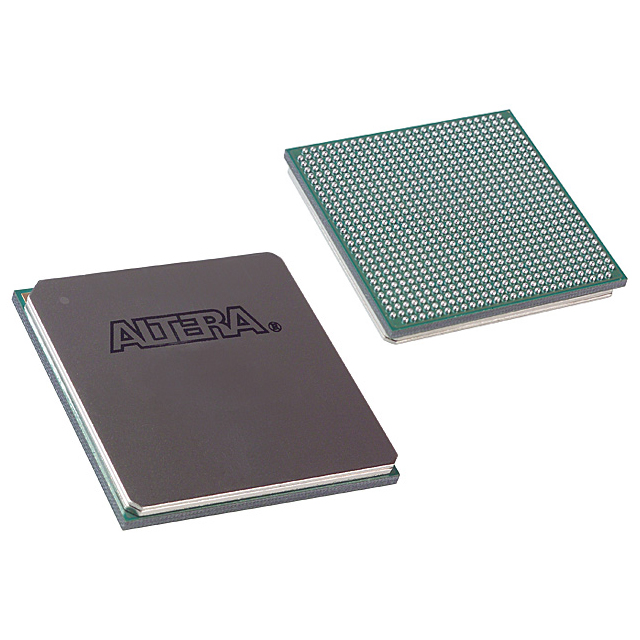
Overview of EP2SGX30DF780C4N – Stratix® II GX FPGA, 780-BBGA, 33,880 LEs
The EP2SGX30DF780C4N is an Intel Stratix® II GX field programmable gate array (FPGA) in a 780-ball BGA package. It is built on the Stratix II GX architecture and is intended for designs that require a high-density logic array, substantial embedded memory, and the family’s high-speed transceiver technology.
Typical use cases include high-speed backplane interfaces, chip-to-chip bridging, and communications protocol applications where scalable logic, abundant I/O, and family-level transceiver capabilities can accelerate time to market.
Key Features
- High-density logic – 33,880 logic elements provide significant programmable logic resources for complex digital designs.
- Embedded memory – Approximately 1.37 Mbits of on-chip RAM for buffers, FIFOs, and local storage.
- I/O resources – 361 user I/O pins support diverse interface requirements across the device.
- Stratix II GX transceiver architecture (family-level) – Leverages Stratix II GX family transceiver technology; the family supports serial data rates from 600 Mbps up to 6.375 Gbps per channel and is designed for high-speed serial protocols (family-level capability).
- Clocking and DSP support (family-level) – Stratix II GX family devices include multiple global and regional clock networks, enhanced PLLs, and dedicated DSP blocks for multiply and FIR implementations (family-level features described in the device family documentation).
- Supply voltage – Operates with a core supply in the 1.15 V to 1.25 V range, enabling designs targeting the Stratix II GX power domain.
- Package and mounting – 780-BBGA package (supplier device package listed as 780-FBGA, 29 × 29 mm) for surface-mount PCB integration.
- Commercial grade & environmental – Commercial temperature grade (0 °C to 85 °C) and RoHS compliant.
Typical Applications
- High-speed backplane interfaces – Use the Stratix II GX family’s transceiver technology and abundant logic to implement backplane protocols and PHY bridging.
- Chip-to-chip bridging – High I/O count and programmable logic enable protocol conversion and high-throughput chip-to-chip links.
- Communications protocol processing – On-chip memory and DSP/clocking features (family-level) support packet buffering, framing, and protocol handling.
- High-performance embedded systems – Dense logic and embedded RAM allow complex control, signal processing, and interface aggregation in compact board-level designs.
Unique Advantages
- Substantial programmable capacity: 33,880 logic elements provide headroom for complex state machines, datapaths, and custom accelerators.
- Significant embedded memory: Approximately 1.37 Mbits of on-chip RAM reduces reliance on external memory for mid-sized buffers and FIFOs.
- Large I/O availability: 361 I/O pins offer flexible routing for multiple parallel interfaces and mixed-signal front ends.
- Stratix II GX family capabilities: Access to high-speed serial transceiver architecture and family-level clocking/DSP features helps address demanding communications and interface designs.
- Compact BGA package: 780-ball FBGA (29 × 29 mm) balances a high pin count with a PCB footprint suitable for dense system designs.
- Regulatory-friendly: RoHS compliance supports environmentally conscious manufacturing and supply chain requirements.
Why Choose EP2SGX30DF780C4N?
The EP2SGX30DF780C4N positions designers to take advantage of the Stratix II GX family architecture while providing a high logic capacity, substantial on-chip RAM, and a large complement of I/O. Its commercial temperature rating and RoHS compliance make it suitable for a broad set of embedded and communications applications.
This device is appropriate for engineers building high-throughput interfaces, protocol bridges, or mid-range signal-processing functions who need programmable density, integrated memory, and the option to leverage family-level high-speed transceiver and clocking features described in the Stratix II GX documentation.
Request a quote or submit a pricing inquiry to check availability and receive further purchasing details for EP2SGX30DF780C4N.


Date Founded: 1968
Headquarters: Santa Clara, California, USA
Employees: 130,000+
Revenue: $54.23 Billion
Certifications and Memberships: ISO9001:2015, ISO14001:2015, ISO17025:2017, ISO27001:2022, ISO45001:2018, ISO50001:2018


