
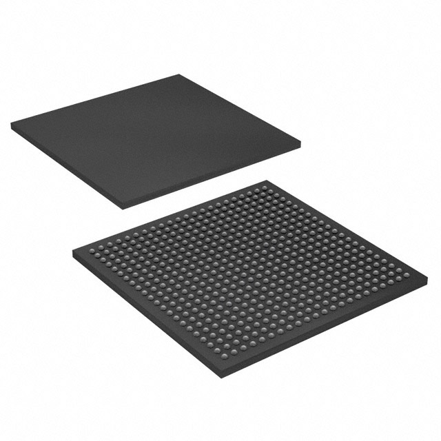
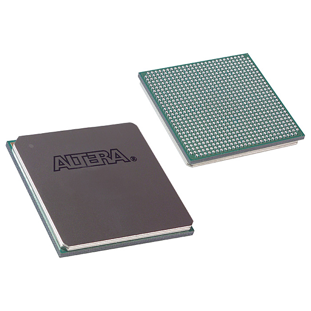
EP2SGX30DF780C5N
| Part Description |
Stratix® II GX Field Programmable Gate Array (FPGA) IC 361 1369728 33880 780-BBGA |
|---|---|
| Quantity | 866 Available (as of June 15, 2026) |

| Product Category | Field Programmable Gate Array (FPGA) |
|---|---|
| Manufacturer | Intel |
| Manufacturing Status | Obsolete |
| Manufacturer Standard Lead Time | Contact Us |
| Datasheet |
Specifications & Environmental
| Device Package | 780-FBGA (29x29) | Grade | Commercial | Operating Temperature | 0°C – 85°C | ||
|---|---|---|---|---|---|---|---|
| Package / Case | 780-BBGA | Number of I/O | 361 | Voltage | 1.15 V - 1.25 V | ||
| Mounting Method | Surface Mount | RoHS Compliance | RoHS Compliant | REACH Compliance | REACH Unaffected | ||
| Moisture Sensitivity Level | 3 (168 Hours) | Number of LABs/CLBs | 1694 | Number of Logic Elements/Cells | 33880 | ||
| Number of Gates | N/A | ECCN | 3A991D | HTS Code | 8542.39.0001 | ||
| Qualification | N/A | Total RAM Bits | 1369728 |
Overview of EP2SGX30DF780C5N – Stratix® II GX FPGA, 33,880 logic elements, 780-BBGA
The EP2SGX30DF780C5N is a Stratix II GX Field Programmable Gate Array (FPGA) offered in a 780-ball BGA package. As a member of the Stratix II GX family, it pairs a scalable, high-performance logic array with the family’s high-speed serial transceiver architecture to support demanding communications and interface applications.
With 33,880 logic elements, approximately 1.37 Mbits of embedded memory, and 361 user I/Os, this commercial-grade, surface-mount FPGA is suited for applications that require significant on-chip logic, memory, and high I/O density while operating within a 0 °C to 85 °C temperature range and a 1.15 V–1.25 V core supply window.
Key Features
- Core Logic 33,880 logic elements and 1,694 logic array blocks provide a large, flexible programmable fabric for complex digital functions and custom processing pipelines.
- Embedded Memory Approximately 1.37 Mbits of on-chip RAM suitable for FIFOs, buffers, and on-chip data storage.
- I/O Density 361 user I/Os delivered in a high-density package to support broad interfacing needs and parallel bus connectivity.
- Stratix II GX Family Transceiver Technology Family-level features include high-speed serial transceivers with clock and data recovery (CDR) and SERDES capability (family supports up to 6.375 Gbps per channel), enabling robust serial link implementations and protocol bridging.
- DSP and Timing Resources Family architecture includes high-speed DSP blocks for multipliers and MAC functions and up to four enhanced PLLs per device for flexible clocking, spread spectrum, and dynamic clock control (family-level capabilities).
- Memory Architecture TriMatrix memory architecture (family feature) with three RAM block sizes supports true dual-port RAM and high-performance FIFOs.
- Package & Mounting 780-ball BBGA package (supplier device package: 780-FBGA, 29×29) in a surface-mount form factor for compact board-level integration.
- Power & Temperature Core supply voltage: 1.15 V to 1.25 V. Operating temperature range: 0 °C to 85 °C (commercial grade).
- Regulatory RoHS compliant.
Typical Applications
- High-Speed Communications Implement serial link endpoints and protocol bridging where family transceiver capabilities and CDR/SERDES support are required.
- Backplane and Chip-to-Chip Interfaces Use the device’s high I/O count and Stratix II GX family transceiver technology to implement backplane interfaces and high-bandwidth chip-to-chip links.
- Custom Data Processing Leverage the large logic element count and on-chip memory for packet processing, buffering, and application-specific acceleration using DSP resources.
- Memory Interface Systems Integrate with external high-speed memory standards supported by the family architecture for data buffering and throughput-intensive designs.
Unique Advantages
- High Logic Capacity: 33,880 logic elements provide substantial programmable resources for complex state machines, custom processors, and parallel datapaths.
- Significant On-Chip Memory: Approximately 1.37 Mbits of embedded RAM reduces external memory dependence for FIFOs and temporary storage.
- Broad I/O Count: 361 user I/Os enable dense interfacing to peripherals, buses, and daughter-card connectors without excessive PCB routing complexity.
- Stratix II GX Transceiver Ecosystem: Family transceiver features (CDR, SERDES, high data-rate support) allow designs targeting modern serial protocols and flexible link reconfiguration.
- Compact, Surface-Mount Package: 780-BBGA (780-FBGA, 29×29) balances high pin count with a compact footprint for space-constrained boards.
- Commercial Temperature and RoHS Compliance: Rated 0 °C to 85 °C and RoHS-compliant for standard commercial deployments and regulatory conformity.
Why Choose EP2SGX30DF780C5N?
The EP2SGX30DF780C5N combines a large logic fabric, substantial embedded memory, and a high pin-count I/O interface in a compact BGA package, delivering a balanced solution for communications, interface bridging, and custom data-processing designs. As part of the Stratix II GX family, it benefits from family-level transceiver, DSP, and memory architecture features that accelerate development of high-bandwidth applications.
This device is well-suited for design teams that require scalable logic capacity, flexible on-chip memory, and the ability to implement serial and parallel interfaces within commercial temperature bounds while maintaining RoHS compliance.
Request a quote or submit an inquiry to receive pricing, availability, and technical support information for EP2SGX30DF780C5N.


Date Founded: 1968
Headquarters: Santa Clara, California, USA
Employees: 130,000+
Revenue: $54.23 Billion
Certifications and Memberships: ISO9001:2015, ISO14001:2015, ISO17025:2017, ISO27001:2022, ISO45001:2018, ISO50001:2018


