
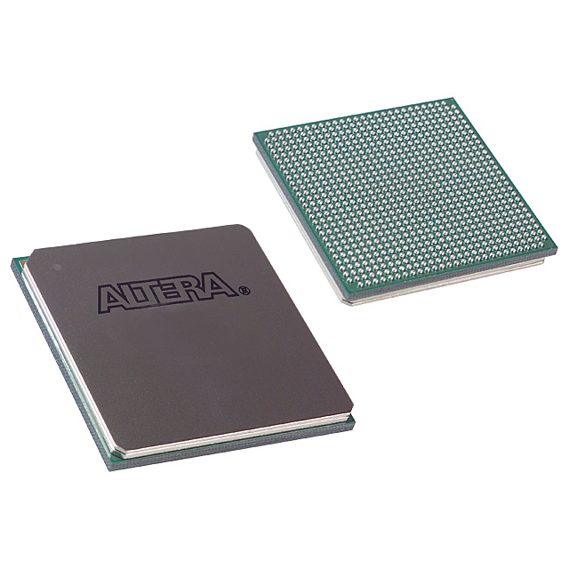
EP2SGX30DF780I4N
| Part Description |
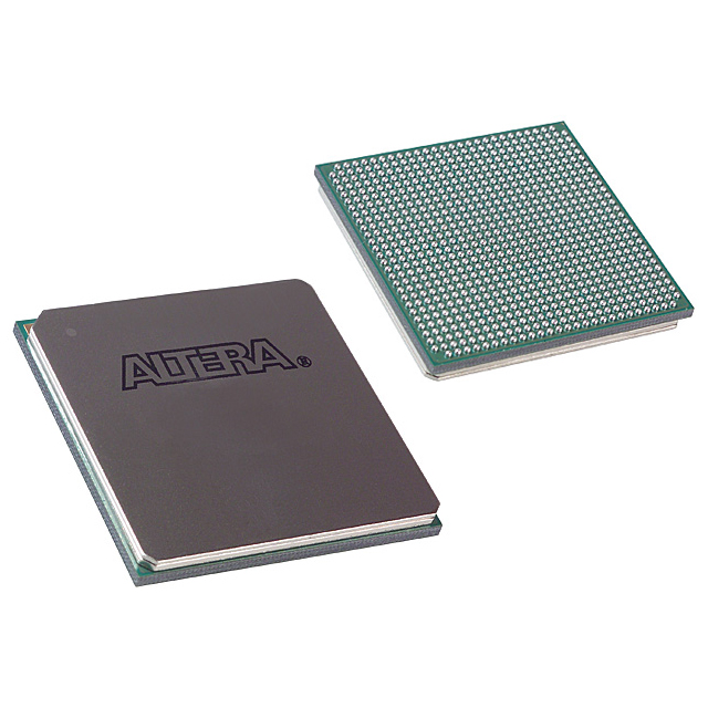
Stratix® II GX Field Programmable Gate Array (FPGA) IC 361 1369728 33880 780-BBGA |
|---|---|
| Quantity | 1,875 Available (as of October 7, 2026) |
| Product Category | Field Programmable Gate Array (FPGA) |
|---|---|
| Manufacturer | Intel |
| Manufacturing Status | Obsolete |
| Manufacturer Standard Lead Time | Contact Us |
| Datasheet |
Specifications & Environmental
| Device Package | 780-FBGA (29x29) | Grade | Industrial | Operating Temperature | -40°C – 100°C | ||
|---|---|---|---|---|---|---|---|
| Package / Case | 780-BBGA | Number of I/O | 361 | Voltage | 1.15 V - 1.25 V | ||
| Mounting Method | Surface Mount | RoHS Compliance | RoHS Compliant | REACH Compliance | REACH Unaffected | ||
| Moisture Sensitivity Level | 3 (168 Hours) | Number of LABs/CLBs | 1694 | Number of Logic Elements/Cells | 33880 | ||
| Number of Gates | N/A | ECCN | 3A991D | HTS Code | 8542.39.0001 | ||
| Qualification | N/A | Total RAM Bits | 1369728 |
Overview of EP2SGX30DF780I4N – Stratix® II GX FPGA, 780‑BBGA
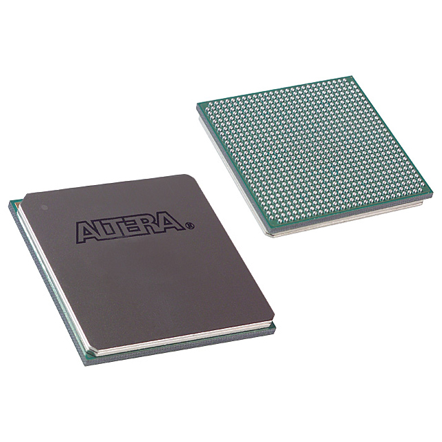
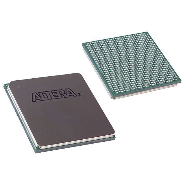
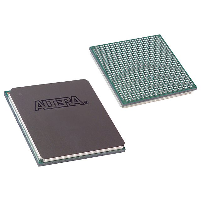
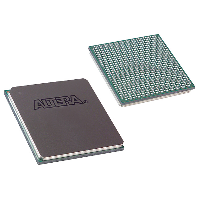
The EP2SGX30DF780I4N is a Stratix® II GX family field‑programmable gate array (FPGA) manufactured by Intel. It combines a high‑performance logic array with the Stratix II GX family’s high‑speed serial transceiver architecture to address demanding communications and interface applications.
With 33,880 logic elements and approximately 1.37 Mbits of embedded RAM, this device targets designs that require significant on‑chip logic and memory, broad I/O density, and industrial temperature operation. Family features include scalable transceiver capability, DSP resources, and rich clocking options to support protocol bridging, backplane interfaces, and high‑speed links.
Key Features
- Logic Density — 33,880 logic elements for implementing complex custom logic and control functions.
- Embedded Memory — Approximately 1.37 Mbits of on‑chip RAM to implement FIFOs, buffers, and local storage.
- I/O Capacity — 361 device I/O pins with support for numerous single‑ended and differential I/O standards (family support), enabling broad interfacing options.
- High‑Speed Transceivers (family) — Stratix II GX family transceiver technology provides clock and data recovery and SERDES capability with data rates up to 6.375 Gbps and configurable channel operation for serial protocol support.
- DSP & Clocking (family) — High‑speed DSP blocks and up to four enhanced PLLs per device (family features) support multiply/accumulate operations and advanced clock management.
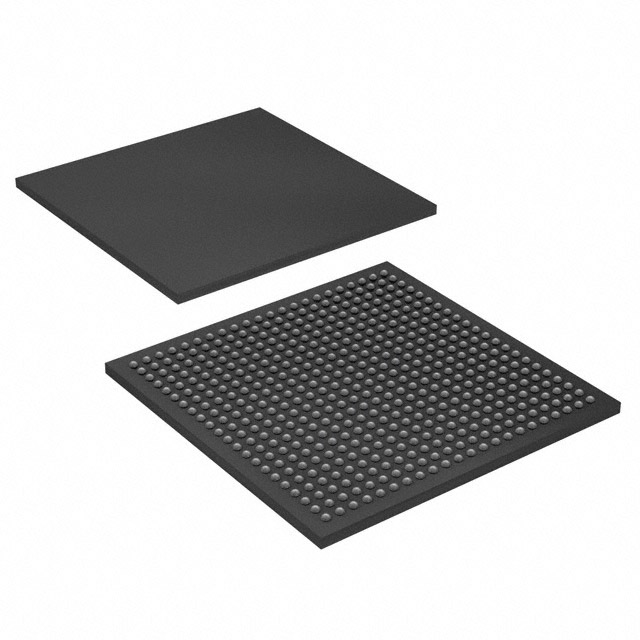
- Package & Mounting — 780‑BBGA package (supplier device package: 780‑FBGA, 29×29) in a surface‑mount form factor for compact board integration.
- Power & Operating Range — Core supply range 1.15 V to 1.25 V and industrial operating temperature from −40 °C to 100 °C.
- Security & Configuration (family) — Family support for configuration bitstream encryption and remote configuration updates to help protect design IP and enable field reconfiguration.
- RoHS Compliant — Device meets RoHS requirements for reduced hazardous substances.
Typical Applications
- High‑Speed Communications — Implements multi‑Gbps serial links and protocol bridging using the Stratix II GX family transceiver capabilities and on‑chip SERDES.
- Networking & Telecom — Backplane interfaces, packet buffering, and interface conversion leveraging the device’s logic density, embedded RAM, and I/O count.
- Video & Broadcast Systems — Support for high‑bandwidth serial protocols and deterministic data paths suitable for video transport and SDI‑class links (family transceiver support).
- DSP & Signal Processing — Use high‑speed DSP blocks and internal memory for filtering, accumulation, and real‑time signal processing tasks.
- Custom SoC & Prototyping — Reconfigurable logic and abundant I/O make the device suitable for prototyping and implementing custom system functions and accelerators.
Unique Advantages
- High logic capacity: 33,880 logic elements enable substantial custom digital functionality without external glue logic.
- Significant on‑chip memory: Approximately 1.37 Mbits of embedded RAM reduces dependence on external memory for buffering and FIFOs.
- Broad I/O density: 361 I/O pins provide flexibility for wide buses, multiple interfaces, and board‑level partitioning.
- Industrial temperature rating: Specified operation from −40 °C to 100 °C supports deployments in harsh and industrial environments.
- Flexible package options: 780‑BBGA/780‑FBGA (29×29) surface‑mount package supports compact board designs with high pin count.
- Family transceiver and DSP ecosystem: Stratix II GX family features such as high‑speed transceivers, DSP blocks, and enhanced PLLs simplify implementation of high‑performance serial and signal processing designs.
Why Choose EP2SGX30DF780I4N?
The EP2SGX30DF780I4N brings together substantial logic and embedded memory with the Stratix II GX family’s high‑speed transceiver and DSP capabilities, offering a balanced platform for communications, networking, video, and DSP‑focused designs. Its industrial temperature rating and high I/O count make it suitable for robust, production‑grade systems that require reliable operation across a wide thermal range.
Designers benefit from a mature family architecture that supports advanced clocking, transceiver configuration, and Altera MegaCore/AMPP megafunctions described in the Stratix II GX documentation, providing avenues for faster integration and long‑term design scalability.
Request a quote or submit an inquiry to receive pricing, availability, and additional technical information for EP2SGX30DF780I4N.





















Date Founded: 1968
Headquarters: Santa Clara, California, USA
Employees: 130,000+
Revenue: $54.23 Billion
Certifications and Memberships: ISO9001:2015, ISO14001:2015, ISO17025:2017, ISO27001:2022, ISO45001:2018, ISO50001:2018


