
EP2SGX60CF780C3
| Part Description |
Stratix® II GX Field Programmable Gate Array (FPGA) IC 364 2544192 60440 780-BBGA |
|---|---|
| Quantity | 1,168 Available (as of June 14, 2026) |

| Product Category | Field Programmable Gate Array (FPGA) |
|---|---|
| Manufacturer | Intel |
| Manufacturing Status | Obsolete |
| Manufacturer Standard Lead Time | Contact Us |
| Datasheet |
Specifications & Environmental
| Device Package | 780-FBGA (29x29) | Grade | Commercial | Operating Temperature | 0°C – 85°C | ||
|---|---|---|---|---|---|---|---|
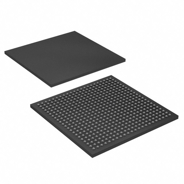
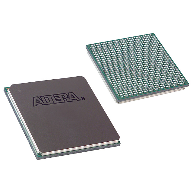
| Package / Case | 780-BBGA | Number of I/O | 364 | Voltage | 1.15 V - 1.25 V | ||
| Mounting Method | Surface Mount | RoHS Compliance | RoHS non-compliant | REACH Compliance | REACH Unaffected | ||
| Moisture Sensitivity Level | 3 (168 Hours) | Number of LABs/CLBs | 3022 | Number of Logic Elements/Cells | 60440 | ||
| Number of Gates | N/A | ECCN | 3A991D | HTS Code | 8542.39.0001 | ||
| Qualification | N/A | Total RAM Bits | 2544192 |
Overview of EP2SGX60CF780C3 – Stratix II GX FPGA, 60,440 logic elements, 780-BBGA
The EP2SGX60CF780C3 is a Stratix® II GX field programmable gate array (FPGA) offered in a 780-BBGA package. It delivers a scalable, high-performance logic array with substantial embedded memory and a large I/O count for complex digital designs.
Designed for applications that require high-bandwidth interfacing and flexible logic integration, the device combines the Stratix II GX series architecture with features such as on-chip RAM, DSP resources, and family-level high-speed serial transceiver technology to support communication and protocol-bridging tasks.
Key Features
- Logic Capacity — 60,440 logic elements providing a large programmable fabric for complex logic and control functions.
- Logic Array Blocks — 3,022 logic array blocks supporting scalable logic partitioning and resource allocation.
- Embedded Memory — Approximately 2.54 Mbits of on-chip RAM (2,544,192 bits) for FIFOs, buffers, and small on-chip storage needs.
- I/O Count — 364 I/O pins to support wide parallel interfaces and mixed-signal board-level connectivity.
- Stratix II GX Family Transceiver Capabilities — Family-level support for high-speed serial transceivers with data rates up to 6.375 Gbps and features such as clock and data recovery, adaptive equalization, and dynamic reconfiguration.
- DSP and Memory Architecture — Series features include high-speed DSP blocks and TriMatrix memory (three RAM block sizes) for high-performance arithmetic, FIR filtering, and dual-port memory implementations.
- Programmable Clocking — Up to four enhanced PLLs per device (series feature) enabling spread-spectrum, bandwidth programming, and phase shifting for complex clocking schemes.
- Power and Supply — Core voltage supply range of 1.15 V to 1.25 V to match system power rails and design constraints.
- Package — 780-BBGA (supplier device package: 780-FBGA, 29 × 29) tailored for surface-mount board integration.
- Commercial Grade — Operating temperature range from 0 °C to 85 °C suitable for commercial electronics applications.
- RoHS Compliant — Meets RoHS environmental requirements for restricted substances.
Typical Applications
- High-speed Communications — Use in backplane interfaces and protocol bridging where the series’ transceiver technology and high logic density enable serial-to-parallel and protocol conversion tasks.
- Chip-to-Chip Interconnects — Implement high-bandwidth chip-to-chip links and serialization/deserialization with family-level transceiver support.
- Packet Processing and Networking — Packet buffering, classification, and forwarding functions leveraging on-chip RAM and DSP resources.
- Memory Interface Controllers — Control and interface logic for external DDR/QDR memory systems using the device’s abundant I/O and embedded memory resources.
Unique Advantages
- High Logic Integration: 60,440 logic elements enable implementation of large-scale, custom logic subsystems on a single FPGA, reducing board-level complexity.
- Substantial On-chip RAM: Approximately 2.54 Mbits of embedded memory for efficient FIFO, buffer, and dual-port memory implementations without relying solely on external RAM.
- Extensive I/O Density: 364 I/Os support wide parallel interfaces and multiple peripheral connections, simplifying board routing and system architecture.
- Family-Level High-speed Serial Capability: Stratix II GX transceiver features (up to 6.375 Gbps) provide the ability to handle modern serial protocols and dynamic reconfiguration options.
- Flexible Clocking and DSP Support: Enhanced PLLs and dedicated DSP resources (series features) allow high-performance arithmetic and multi-rate clock domains for signal processing applications.
- Commercial-ready Packaging: 780-BBGA surface-mount package and a commercial temperature grade make the device suitable for a broad range of production electronic products.
Why Choose EP2SGX60CF780C3?
The EP2SGX60CF780C3 combines substantial programmable logic, embedded memory, and an extensive I/O complement in a compact 780-BBGA package. It is positioned for designs that demand programmable bandwidth, protocol flexibility, and significant on-chip resources without sacrificing board-level density.
Engineers building communication equipment, high-speed interfaces, and complex control logic will find this Stratix II GX device provides the architectural features and series-level transceiver capabilities needed for scalable, performance-oriented designs while benefiting from RoHS compliance and commercial-grade operating conditions.
Request a quote or submit an inquiry for pricing and availability to move your design forward with the EP2SGX60CF780C3.


Date Founded: 1968
Headquarters: Santa Clara, California, USA
Employees: 130,000+
Revenue: $54.23 Billion
Certifications and Memberships: ISO9001:2015, ISO14001:2015, ISO17025:2017, ISO27001:2022, ISO45001:2018, ISO50001:2018


