
EP2SGX60CF484I4
| Part Description |
Stratix® II GX Field Programmable Gate Array (FPGA) IC 291 2544192 60440 484-BBGA |
|---|---|
| Quantity | 336 Available (as of June 15, 2026) |
| Product Category | Field Programmable Gate Array (FPGA) |
|---|---|
| Manufacturer | Intel |
| Manufacturing Status | Obsolete |
| Manufacturer Standard Lead Time | Contact Us |
| Datasheet |
Specifications & Environmental
| Device Package | 484-FBGA (23x23) | Grade | Industrial | Operating Temperature | -40°C – 100°C | ||
|---|---|---|---|---|---|---|---|
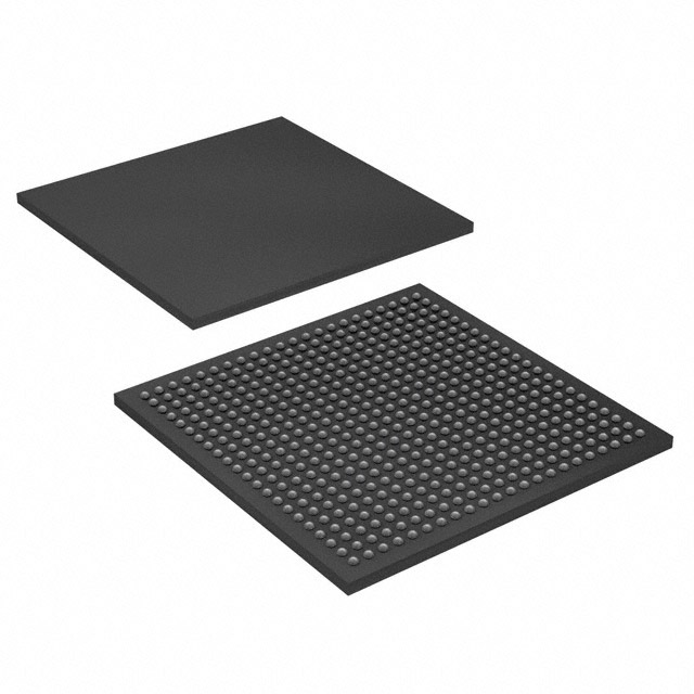
| Package / Case | 484-BBGA | Number of I/O | 291 | Voltage | 1.15 V - 1.25 V | ||
| Mounting Method | Surface Mount | RoHS Compliance | Unknown | REACH Compliance | REACH Unaffected | ||
| Moisture Sensitivity Level | 3 (168 Hours) | Number of LABs/CLBs | 3022 | Number of Logic Elements/Cells | 60440 | ||
| Number of Gates | N/A | ECCN | 3A001A2C | HTS Code | 8542.39.0001 | ||
| Qualification | N/A | Total RAM Bits | 2544192 |
Overview of EP2SGX60CF484I4 – Stratix® II GX FPGA, 60,440 Logic Elements, 484‑BBGA
The EP2SGX60CF484I4 is a Stratix® II GX field‑programmable gate array (FPGA) in a 484‑BBGA package intended for industrial applications. It combines a high‑performance logic array with on‑chip memory and the Stratix II GX family’s high‑speed transceiver and clocking architecture for demanding communications and data‑processing designs.
With 60,440 logic elements, approximately 2.54 Mbits of embedded memory, and 291 I/O pins, this device targets high‑bandwidth system functions such as backplane interfaces, chip‑to‑chip links, and communications protocol bridging where integration, deterministic timing, and industrial temperature support are required.
Key Features
- Logic Capacity — 60,440 logic elements provide the programmable fabric for complex control, processing, and interface logic.
- Embedded Memory — Approximately 2.54 Mbits of on‑chip RAM and the Stratix TriMatrix memory architecture support true dual‑port memories and high‑performance FIFOs.
- I/O Density — 291 I/O pins enable broad interfacing options for parallel buses, control signals, and high‑speed serial blocks.
- High‑Speed Transceivers (Series Capability) — Stratix II GX family transceiver technology supports serial data rates from 600 Mbps to 6.375 Gbps, with features such as clock and data recovery (CDR), programmable pre‑emphasis, adaptive equalization, and per‑channel power‑down for link power management.
- DSP and Performance Blocks — Integrated high‑speed DSP resources and dedicated multipliers support multiply‑accumulate and FIR filter implementations (documented up to 450 MHz in the series).
- Clocking and PLLs — Up to four enhanced PLLs per device in the series provide programmable bandwidth, spread‑spectrum support, clock switch‑over and real‑time reconfiguration for flexible clock management.
- Memory Interface Support (Series Capability) — Series documentation cites support for external memories including QDR/QDRII, DDR/DDR2 SDRAM and SDR SDRAM for high‑throughput memory subsystems.
- Power and Supply — Core supply range 1.15 V to 1.25 V, with transceiver dynamic settings for output differential voltage (VOD) and per‑channel power control.
- Package and Mounting — 484‑BBGA (supplier package referenced as 484‑FBGA 23×23) in surface‑mount format for compact board integration.
- Industrial Temperature and Compliance — Rated for operation from −40 °C to 100 °C and RoHS compliant for industrial deployments.
- Configuration & Security (Series Capability) — Series documentation describes support for configuration bitstream encryption and remote configuration updates.
Typical Applications
- Telecommunications & Networking — Implements high‑speed serial links and protocol bridging for backplanes, line cards, and packet processing.
- Data Center and Interconnect — Handles chip‑to‑chip interfaces and memory‑centric designs requiring large logic capacity and high I/O density.
- Signal Processing — Leverages on‑chip DSP resources and embedded RAM for filtering, aggregation, and real‑time data manipulation.
- Embedded Systems in Industrial Environments — Industrial temperature rating and surface‑mount package enable deployment in factory automation, instrumentation, and control systems.
Unique Advantages
- High Logic and Memory Integration: Combines 60,440 logic elements with approximately 2.54 Mbits of embedded RAM to consolidate functions that would otherwise require multiple devices.
- Advanced Serial Capabilities: Stratix II GX transceiver technology supports multi‑Gbps serial links, configurable equalization and pre‑emphasis, and per‑channel power management for adaptable link design.
- Flexible Clocking: Multiple enhanced PLLs and extensive clock networks (series documentation) provide deterministic timing and support complex clock domains.
- Industrial‑Grade Operation: Rated for −40 °C to 100 °C, making it suitable for deployment in demanding temperature environments.
- Broad Memory and Interface Support: Series-level support for DDR/DDR2/QDR families and numerous I/O standards helps streamline board‑level memory and interface design.
- Surface‑Mount, High‑Density Package: 484‑BBGA (484‑FBGA 23×23) enables compact board layouts while exposing high I/O counts for system integration.
Why Choose EP2SGX60CF484I4?
The EP2SGX60CF484I4 positions itself as a high‑capacity, industrial‑rated Stratix II GX FPGA that brings together substantial programmable logic, embedded memory, and the series’ high‑speed transceiver and clocking capabilities. Its combination of logic density, IO count, and industrial temperature range makes it well suited to communications, data‑processing, and embedded industrial designs that demand integration and deterministic performance.
For engineering teams building scalable systems, the device offers architecture and features—documented across the Stratix II GX family—that simplify implementation of high‑bandwidth links, memory interfaces, and DSP tasks while enabling controlled power and clocking strategies.
Request a quote or submit an RFQ to start procurement and evaluate the EP2SGX60CF484I4 for your next high‑performance FPGA design.


Date Founded: 1968
Headquarters: Santa Clara, California, USA
Employees: 130,000+
Revenue: $54.23 Billion
Certifications and Memberships: ISO9001:2015, ISO14001:2015, ISO17025:2017, ISO27001:2022, ISO45001:2018, ISO50001:2018


