
EP2SGX30DF780C5
| Part Description |
Stratix® II GX Field Programmable Gate Array (FPGA) IC 361 1369728 33880 780-BBGA |
|---|---|
| Quantity | 620 Available (as of June 15, 2026) |

| Product Category | Field Programmable Gate Array (FPGA) |
|---|---|
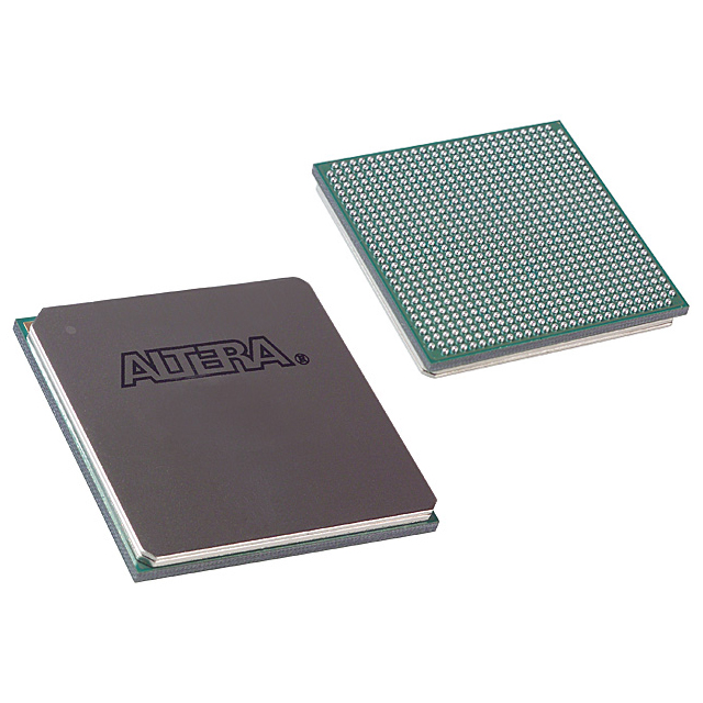
| Manufacturer | Intel |
| Manufacturing Status | Obsolete |
| Manufacturer Standard Lead Time | Contact Us |
| Datasheet |
Specifications & Environmental
| Device Package | 780-FBGA (29x29) | Grade | Commercial | Operating Temperature | 0°C – 85°C | ||
|---|---|---|---|---|---|---|---|
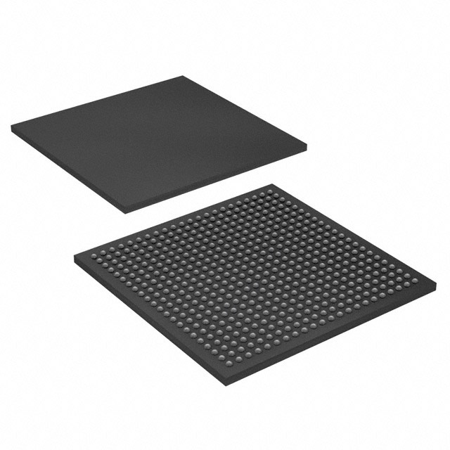
| Package / Case | 780-BBGA | Number of I/O | 361 | Voltage | 1.15 V - 1.25 V | ||
| Mounting Method | Surface Mount | RoHS Compliance | RoHS non-compliant | REACH Compliance | REACH Unaffected | ||
| Moisture Sensitivity Level | 3 (168 Hours) | Number of LABs/CLBs | 1694 | Number of Logic Elements/Cells | 33880 | ||
| Number of Gates | N/A | ECCN | 3A991D | HTS Code | 8542.39.0001 | ||
| Qualification | N/A | Total RAM Bits | 1369728 |
Overview of EP2SGX30DF780C5 – Stratix® II GX FPGA, 780-BBGA package
The EP2SGX30DF780C5 is a Stratix® II GX field-programmable gate array (FPGA) in a 780-BBGA surface-mount package. It combines a high-performance logic array with the Stratix II GX family architecture that integrates advanced memory, DSP, and high-speed serial transceiver technologies.
Targeted for communication and high-speed interface designs, this commercial-grade device provides a balance of logic capacity, embedded memory, and I/O density for applications such as backplane interfaces, chip-to-chip links, and protocol bridging.
Key Features
- Logic Capacity — 33,880 logic elements to implement complex digital functions and custom logic blocks.
- Embedded Memory — Approximately 1.37 Mbits of on-chip RAM for FIFOs, buffers, and packet or frame storage.
- I/O Density — 361 user I/O pins, supporting a wide range of system interfacing and parallel bus implementations.
- Stratix II GX Family Transceiver Architecture — Family-level transceiver and SERDES features, including clock and data recovery and support for high-speed serial protocols, provide a foundation for multi-Gbps serial links (see family datasheet for details).
- DSP & Clock Resources — Family architecture includes high-speed DSP blocks and multiple global/regional clock networks to support high-throughput signal processing and synchronized system timing (refer to series documentation for block counts and capabilities).
- Package & Mounting — 780-BBGA (supplier device package: 780-FBGA, 29 × 29 mm) surface-mount package for compact, board-level integration.
- Power & Operating Range — Core voltage supply range of 1.15 V to 1.25 V with an operating temperature range of 0 °C to 85 °C (commercial grade).
- Regulatory — RoHS compliant.
Typical Applications
- High-Speed Backplane Interfaces — Use the Stratix II GX family’s serial and parallel resources to implement multi-lane backplane links and protocol bridging.
- Chip-to-Chip Connectivity — Leverage abundant I/O and family transceiver features for high-throughput board-to-board or chip-to-chip data paths.
- Communications Protocol Bridging — Implement protocol conversion and aggregation where on-chip memory and DSP blocks handle buffering and data manipulation.
- High-Performance Logic and DSP — Deploy the device’s logic elements and embedded memory for packet processing, signal conditioning, or custom hardware acceleration.
Unique Advantages
- Substantial Logic Density: 33,880 logic elements enable implementation of large custom logic designs without external ASICs.
- On-Chip Memory for Real-Time buffering: Approximately 1.37 Mbits of embedded RAM reduces external memory dependence for many FIFO and buffering tasks.
- High I/O Count: 361 I/O pins provide flexibility for wide parallel buses, multiple interfaces, and mixed-signal front-ends.
- Family-Level Serial Capability: Stratix II GX architecture includes high-speed transceiver features suitable for multi-gigabit serial protocols (see series documentation for supported rates and protocols).
- Compact BGA Package: 780-FBGA (29 × 29 mm) package balances board-space efficiency with thermal and routing considerations for dense designs.
- Commercial-Grade Reliability: 0 °C to 85 °C operating range and RoHS compliance make the device suitable for mainstream commercial and communications equipment.
Why Choose EP2SGX30DF780C5?
The EP2SGX30DF780C5 positions itself as a versatile Stratix II GX family member for designers who need a significant logic footprint, substantial embedded memory, and a high I/O count in a compact BGA package. Its architecture and family-level transceiver capabilities make it well suited for communications, protocol bridging, and high-throughput data-path applications.
For teams focused on scalable, field-programmable solutions, this device offers long-term design flexibility supported by the Stratix II GX documentation and Intel manufacturing pedigree—helpful when evolving product requirements call for higher integration or reconfiguration without a full hardware redesign.
Request a quote or submit a sales inquiry to get pricing, availability, and additional integration information for EP2SGX30DF780C5.


Date Founded: 1968
Headquarters: Santa Clara, California, USA
Employees: 130,000+
Revenue: $54.23 Billion
Certifications and Memberships: ISO9001:2015, ISO14001:2015, ISO17025:2017, ISO27001:2022, ISO45001:2018, ISO50001:2018


