
EP2SGX30DF780I4
| Part Description |
Stratix® II GX Field Programmable Gate Array (FPGA) IC 361 1369728 33880 780-BBGA |
|---|---|
| Quantity | 885 Available (as of June 15, 2026) |

| Product Category | Field Programmable Gate Array (FPGA) |
|---|---|
| Manufacturer | Intel |
| Manufacturing Status | Obsolete |
| Manufacturer Standard Lead Time | Contact Us |
| Datasheet |
Specifications & Environmental
| Device Package | 780-FBGA (29x29) | Grade | Industrial | Operating Temperature | -40°C – 100°C | ||
|---|---|---|---|---|---|---|---|
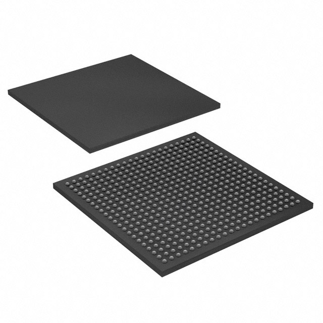
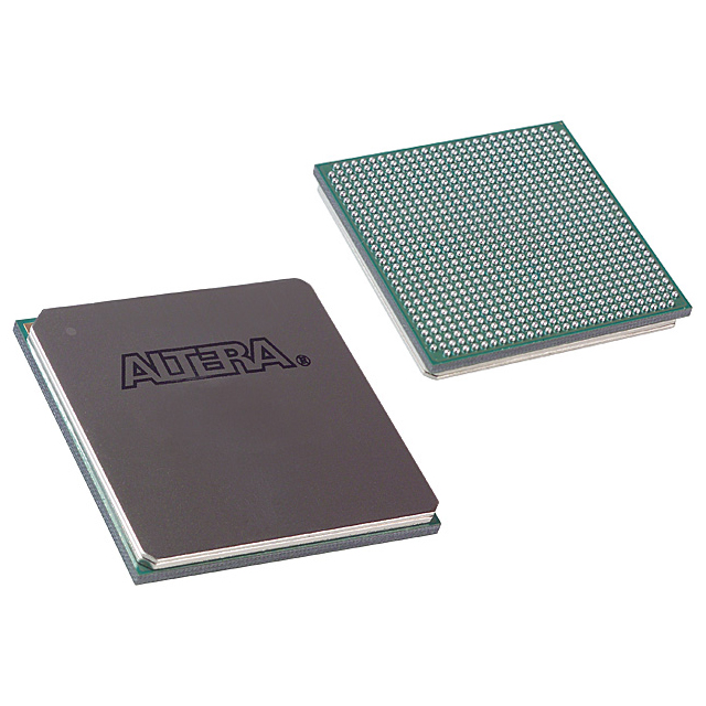
| Package / Case | 780-BBGA | Number of I/O | 361 | Voltage | 1.15 V - 1.25 V | ||
| Mounting Method | Surface Mount | RoHS Compliance | RoHS non-compliant | REACH Compliance | REACH Unaffected | ||
| Moisture Sensitivity Level | 3 (168 Hours) | Number of LABs/CLBs | 1694 | Number of Logic Elements/Cells | 33880 | ||
| Number of Gates | N/A | ECCN | 3A991D | HTS Code | 8542.39.0001 | ||
| Qualification | N/A | Total RAM Bits | 1369728 |
Overview of EP2SGX30DF780I4 – Stratix® II GX FPGA, 33,880 logic elements, 780-BBGA
The EP2SGX30DF780I4 is a Stratix® II GX family Field Programmable Gate Array (FPGA) in a 780-ball BGA package. It pairs a scalable, high-performance logic array with the Stratix II GX family’s high-speed serial transceiver architecture for demanding digital, communications, and protocol-bridging designs.
Targeted at industrial applications, this device offers 33,880 logic elements, approximately 1.37 Mbits of embedded memory, and up to 361 I/O pins, delivering the integration and I/O density needed for backplane interfaces, chip-to-chip links, and high-speed communications tasks.
Key Features
- Logic Capacity — 33,880 logic elements for complex digital designs and system integration.
- Embedded Memory — Approximately 1.37 Mbits of on-chip RAM to implement FIFOs, dual-port memories, and buffering.
- I/O Density — 361 I/Os to support broad interfacing and high pin-count connectivity.
- Stratix II GX Transceiver Architecture — Family-level support for high-speed serial transceivers with clock and data recovery and embedded SERDES; transceivers in the family support data rates up to 6.375 Gbps and device variants with 4–20 channels (family-level capability).
- Programmable Supply Range — Core voltage supply range from 1.15 V to 1.25 V for predictable power budgeting.
- Package & Mounting — 780-ball FBGA (29 × 29 mm) package, surface-mount mounting for compact board integration.
- Industrial Temperature Range — Rated for operation from −40 °C to 100 °C to meet industrial-environment requirements.
- Standards & Interfaces — Family documentation shows support for multiple serial protocols and high-speed external memory interfaces (family-level features include support for PCI Express, Gigabit Ethernet, QDR, DDR, DDR2 and others as described in the Stratix II GX handbook).
- Compliance — RoHS compliant.
Typical Applications
- High-Speed Backplane Interfaces — Use the device’s high I/O density and family-level transceiver performance to implement backplane bridging and switching functions.
- Chip-to-Chip Communication — Leverage the Stratix II GX serial transceiver architecture to handle high-bandwidth, low-latency links between chips or modules.
- Communications Protocol Bridging — Implement protocol conversion and multi-protocol interfaces using the device’s programmable logic, embedded memory, and transceiver capabilities (family-level supported protocols documented in the datasheet).
- High-Speed Memory Interfaces — Pair on-chip RAM and the FPGA fabric to manage external memory interfaces supported at the family level, including QDR and DDR variants.
Unique Advantages
- Substantial Logic & Memory Integration: 33,880 logic elements and ~1.37 Mbits of embedded memory reduce external components and simplify system design.
- High I/O Count: 361 I/Os enable dense connectivity for complex boards and multiple parallel interfaces.
- Family-Level High-Speed Serial Support: Stratix II GX transceiver features (up to 6.375 Gbps, multi-channel capability) enable high-bandwidth serial links where needed.
- Industrial Temperature Rating: −40 °C to 100 °C operation supports deployments in a wide range of industrial environments.
- Compact, Surface-Mount Package: 780-ball FBGA (29 × 29 mm) balances high I/O with a compact footprint for space-constrained designs.
- Standards-Focused Architecture: Family documentation includes support for common high-speed protocols and external memory interfaces to accelerate system integration.
Why Choose EP2SGX30DF780I4?
EP2SGX30DF780I4 places substantial programmable logic, embedded memory, and high I/O density into a single 780-BBGA package, aligning with industrial applications that require robust operation across −40 °C to 100 °C. As part of the Stratix II GX family, it brings a transceiver-capable architecture and family-level support for high-speed serial protocols and external memory interfaces to system designs that demand bandwidth and flexibility.
This device suits customers building high-speed communications, protocol-bridging, and complex interfacing solutions where integration, reliable thermal range, and a scalable FPGA architecture are key to reducing board-level complexity and accelerating time-to-deployment.
Request a quote or submit an inquiry today to get pricing and lead-time information for EP2SGX30DF780I4.


Date Founded: 1968
Headquarters: Santa Clara, California, USA
Employees: 130,000+
Revenue: $54.23 Billion
Certifications and Memberships: ISO9001:2015, ISO14001:2015, ISO17025:2017, ISO27001:2022, ISO45001:2018, ISO50001:2018


