
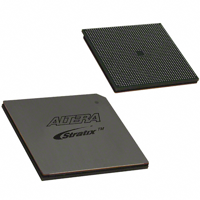
EP2SGX130GF1508C4
| Part Description |
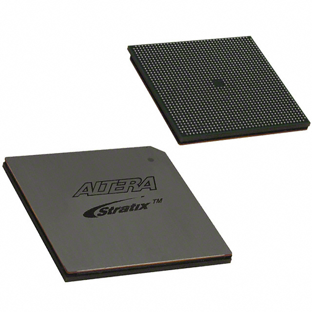
Stratix® II GX Field Programmable Gate Array (FPGA) IC 734 6747840 132540 1508-BBGA, FCBGA |
|---|---|
| Quantity | 222 Available (as of October 7, 2026) |
| Product Category | Field Programmable Gate Array (FPGA) |
|---|---|
| Manufacturer | Intel |
| Manufacturing Status | Obsolete |
| Manufacturer Standard Lead Time | Contact Us |
| Datasheet |
Specifications & Environmental
| Device Package | 1508-FBGA, FC (40x40) | Grade | Commercial | Operating Temperature | 0°C – 85°C | ||
|---|---|---|---|---|---|---|---|
| Package / Case | 1508-BBGA, FCBGA | Number of I/O | 734 | Voltage | 1.15 V - 1.25 V | ||
| Mounting Method | Surface Mount | RoHS Compliance | RoHS non-compliant | REACH Compliance | REACH Unaffected | ||
| Moisture Sensitivity Level | 3 (168 Hours) | Number of LABs/CLBs | 6627 | Number of Logic Elements/Cells | 132540 | ||
| Number of Gates | N/A | ECCN | 3A001A7A | HTS Code | 8542.39.0001 | ||
| Qualification | N/A | Total RAM Bits | 6747840 |
Overview of EP2SGX130GF1508C4 – Stratix® II GX FPGA, 132,540 logic elements, 1508-BBGA
The EP2SGX130GF1508C4 is a Stratix® II GX field-programmable gate array (FPGA) supplied in a 1508-BBGA (FCBGA, 40×40) surface-mount package. It delivers a high logic-density fabric with 132,540 logic elements and approximately 6.75 Mbits of embedded RAM to support complex digital systems and large on-chip buffering.
Built on the Stratix II GX device architecture, the family incorporates high-speed serial transceiver technology, extensive I/O capability and on-chip DSP and clocking resources—making this device suitable for high-speed backplane, chip-to-chip and communications protocol-bridging applications that require dense logic, significant memory and abundant I/O.
Key Features
- Logic Capacity 132,540 logic elements to implement large-scale digital logic and custom processing pipelines.
- Embedded Memory Approximately 6.75 Mbits of on-chip RAM for FIFOs, buffers and block RAM-based storage; the Stratix II GX family uses TriMatrix memory with multiple block sizes for design flexibility.
- I/O Density 734 user I/O pins to support wide buses, parallel interfaces and mixed single-ended/differential signaling.
- High‑Speed Transceiver Technology Stratix II GX family transceivers support 600 Mbps to 6.375 Gbps operation with clock and data recovery (CDR), embedded SERDES and features such as programmable VOD and pre‑emphasis for improved signal integrity.
- DSP and Clocking Resources On-chip high-speed DSP blocks and up to four enhanced PLLs per device family for multiply-accumulate functions, FIR filters, clocking flexibility and real-time PLL reconfiguration.
- Power and Supply Core voltage supply range of 1.15 V to 1.25 V for the device logic array.
- Package & Mounting 1508-BBGA (FCBGA, 40×40) surface-mount package suitable for board-level SMT assembly.
- Operating Range & Compliance Commercial-grade device with operating temperature 0 °C to 85 °C and RoHS compliance.
Typical Applications
- High‑Speed Backplane Interfaces Implements protocol bridging and packet handling where large logic capacity and high I/O counts are required.
- Chip‑to‑Chip Connectivity Provides high-density I/O and transceiver capability for high-throughput, short-reach serial and parallel links between chips and modules.
- Communications Protocol Bridging Stratix II GX transceiver features and embedded DSP make it suitable for protocol conversion, line termination and SERDES-based protocol implementations.
- External Memory Controllers On-chip resources and I/O density support controllers for high‑speed external memories such as DDR/DDR2 and QDR implementations specified by the device family.
Unique Advantages
- High Logic Integration: 132,540 logic elements reduce the need for multiple chips and simplify board-level design.
- Significant On‑Chip Memory: Approximately 6.75 Mbits of embedded RAM enables large buffers and deep FIFOs without external memory.
- Wide I/O Range: 734 I/Os let you implement wide parallel buses and mixed signaling standards on a single device.
- Advanced Transceiver Capability: Family-level support for up to multi-gigabit serial links with CDR and SERDES improves link performance and design flexibility.
- Flexible Clocking and DSP: Enhanced PLLs and DSP blocks support high-performance signal processing and real-time clock management.
- Commercial‑Grade and RoHS‑Compliant: Designed for commercial temperature ranges and environmental compliance for mainstream product lines.
Why Choose EP2SGX130GF1508C4?
The EP2SGX130GF1508C4 combines a high-density logic fabric, substantial embedded memory and a large complement of I/O in a single 1508-BBGA package. Its Stratix II GX architecture provides the transceiver, DSP and clocking features needed for demanding communications and high-throughput applications while enabling compact, integrated designs.
This device is well suited to engineering teams building high-performance interconnects, protocol-bridging modules, memory controllers and other systems requiring a balance of logic capacity, on-chip RAM and transceiver capability, with the long-term support and documentation associated with the Stratix II GX device family.
Request a quote or submit a design inquiry to check availability, pricing and to discuss technical requirements for integrating EP2SGX130GF1508C4 into your next design.





















Date Founded: 1968
Headquarters: Santa Clara, California, USA
Employees: 130,000+
Revenue: $54.23 Billion
Certifications and Memberships: ISO9001:2015, ISO14001:2015, ISO17025:2017, ISO27001:2022, ISO45001:2018, ISO50001:2018


