
EP3C25F256C8
| Part Description |
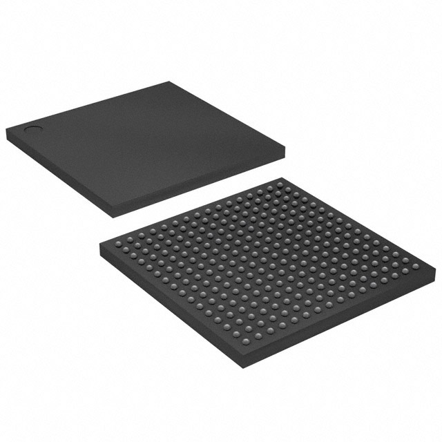
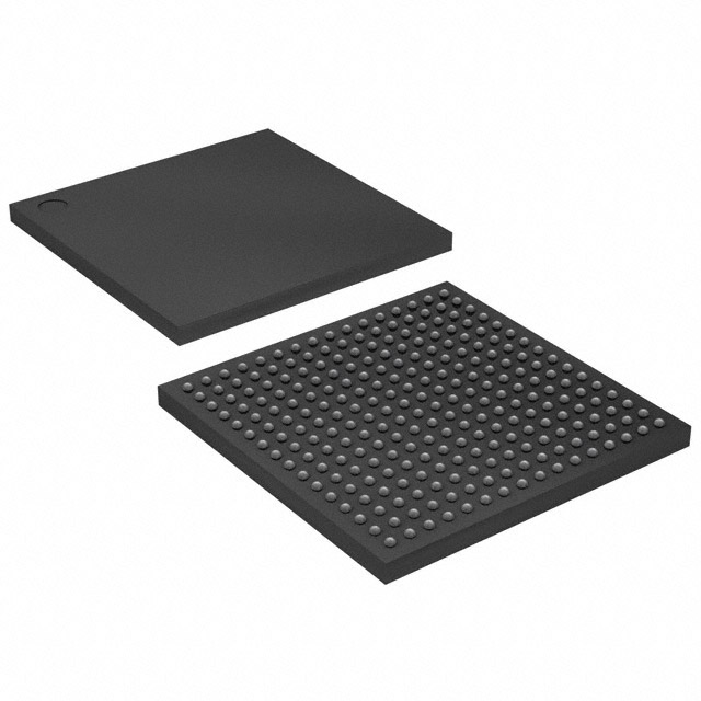
Cyclone® III Field Programmable Gate Array (FPGA) IC 156 608256 24624 256-LBGA |
|---|---|
| Quantity | 1,321 Available (as of October 7, 2026) |

| Product Category | Field Programmable Gate Array (FPGA) |
|---|---|
| Manufacturer | Intel |
| Manufacturing Status | Active |
| Manufacturer Standard Lead Time | 26 Weeks |
| Datasheet |
Specifications & Environmental
| Device Package | 256-FBGA (17x17) | Grade | Commercial | Operating Temperature | 0°C – 85°C | ||
|---|---|---|---|---|---|---|---|
| Package / Case | 256-LBGA | Number of I/O | 156 | Voltage | 1.15 V - 1.25 V | ||
| Mounting Method | Surface Mount | RoHS Compliance | RoHS Compliant | REACH Compliance | REACH Unaffected | ||
| Moisture Sensitivity Level | 3 (168 Hours) | Number of LABs/CLBs | 1539 | Number of Logic Elements/Cells | 24624 | ||
| Number of Gates | N/A | ECCN | 3A991D | HTS Code | 8542.39.0001 | ||
| Qualification | N/A | Total RAM Bits | 608256 |
Overview of EP3C25F256C8 – Cyclone® III Field Programmable Gate Array (FPGA) IC 156 608256 24624 256-LBGA
The EP3C25F256C8 is a Cyclone® III family FPGA offering a low-power, high-functionality programmable fabric for cost-sensitive and high-volume applications. This device combines 24,624 logic elements with approximately 0.61 Mbits of embedded memory (608,256 bits) and 156 user I/Os in a 256-ball LBGA surface-mount package.
Built on a TSMC low-power process and aligned with Cyclone III device family architecture, the EP3C25F256C8 targets designs that require efficient power use, flexible I/O support, and integrated clock and memory resources for embedded control, interface bridging, and system integration tasks.
Key Features
- Programmable Logic 24,624 logic elements suitable for mid-range logic density requirements.
- Embedded Memory Approximately 0.61 Mbits of on-chip RAM (608,256 bits) to support buffering, packet handling, and local data storage.
- I/O Capacity & Flexibility 156 user I/Os with adjustable slew rates and support for a wide range of I/O standards including LVTTL, LVCMOS, SSTL, HSTL, PCI, PCI‑X, LVPECL, BLVDS, LVDS, mini‑LVDS, RSDS, and PPDS.
- Clock Management Four phase-locked loops (PLLs) per device provide clock synthesis and robust clock-domain control for system and interface timing.
- On-Chip Termination & Signal Integrity Multi-value on-chip termination (OCT) calibration and adjustable slew rates help manage PVT variations and improve signal integrity.
- Power & Supply Designed for low-power operation and optimized silicon; core supply range is 1.15 V to 1.25 V.
- Package & Mounting 256-ball LBGA package (supplier package: 256-FBGA 17×17) with surface-mount mounting for compact board-level integration.
- Operating Environment Commercial grade operation from 0 °C to 85 °C.
- Embedded Processor Support Family-level support for the Nios® II embedded processor to enable soft-core embedded processing where applicable.
Typical Applications
- Consumer and Portable Electronics Use the device for interface bridging, local control logic, and timing management where low power and compact packaging matter.
- Embedded Control & Signal Processing Implement custom control algorithms, data path logic, and pre/post-processing with available logic elements and on-chip memory.
- High‑I/O Interface Modules Leverage the broad I/O standard support and 156 I/Os for protocol conversion, multi‑lane interfaces, and I/O-rich subsystems.
- System Integration & Prototyping Rapidly integrate peripherals, clocks, and memory functions within a single device to reduce board-level complexity.
Unique Advantages
- Low-power silicon platform: Designed on a TSMC low-power process to help meet tight power budgets in portable and thermally constrained systems.
- Balanced memory-to-logic ratio: Approximately 0.61 Mbits of embedded RAM paired with 24,624 logic elements enables efficient implementation of data buffering and local storage without external memory in many use cases.
- Robust clocking resources: Four PLLs per device simplify multi-clock domain designs and provide flexible clock synthesis and phase control.
- Broad I/O standard compatibility: Extensive I/O standard support and adjustable slew rates address a wide range of interface requirements and signal integrity needs.
- Compact surface-mount package: 256-LBGA (256-FBGA 17×17) delivers density for space-constrained PCBs while supporting high I/O counts.
- Commercial temperature support: Rated for 0 °C to 85 °C operation for general-purpose and consumer applications.
Why Choose EP3C25F256C8?
The EP3C25F256C8 offers a pragmatic balance of logic capacity, embedded memory, and flexible I/O in a low-power Cyclone III family device. Its combination of 24,624 logic elements, approximately 0.61 Mbits of on-chip RAM, four PLLs, and wide I/O support makes it well suited for mid-range FPGA roles where power efficiency, integration, and predictable thermal behavior are priorities.
This device is appropriate for designers building cost-sensitive, high-volume products that require reliable programmable logic, diverse interface support, and compact packaging. The Cyclone III family heritage and family-level features help ensure a viable upgrade path and ecosystem support for evolving designs.
Request a quote or submit an inquiry to receive pricing and availability information for the EP3C25F256C8.



























Date Founded: 1968
Headquarters: Santa Clara, California, USA
Employees: 130,000+
Revenue: $54.23 Billion
Certifications and Memberships: ISO9001:2015, ISO14001:2015, ISO17025:2017, ISO27001:2022, ISO45001:2018, ISO50001:2018


