
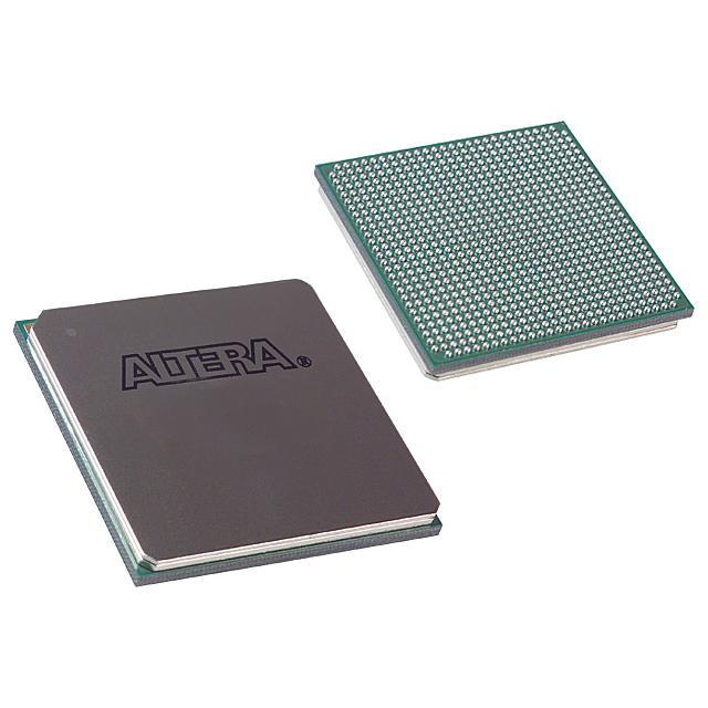
EP3C55U484C6
| Part Description |
Cyclone® III Field Programmable Gate Array (FPGA) IC 327 2396160 55856 484-FBGA |
|---|---|
| Quantity | 1,350 Available (as of June 10, 2026) |

| Product Category | Field Programmable Gate Array (FPGA) |
|---|---|
| Manufacturer | Intel |
| Manufacturing Status | Active |
| Manufacturer Standard Lead Time | 26 Weeks |
| Datasheet |
Specifications & Environmental
| Device Package | 484-UBGA (19x19) | Grade | Commercial | Operating Temperature | 0°C – 85°C | ||
|---|---|---|---|---|---|---|---|
| Package / Case | 484-FBGA | Number of I/O | 327 | Voltage | 1.15 V - 1.25 V | ||
| Mounting Method | Surface Mount | RoHS Compliance | RoHS non-compliant | REACH Compliance | REACH Unaffected | ||
| Moisture Sensitivity Level | 3 (168 Hours) | Number of LABs/CLBs | 3491 | Number of Logic Elements/Cells | 55856 | ||
| Number of Gates | N/A | ECCN | 3A991D | HTS Code | 8542.39.0001 | ||
| Qualification | N/A | Total RAM Bits | 2396160 |
Overview of EP3C55U484C6 – Cyclone® III Field Programmable Gate Array (FPGA) IC, 55,856 Logic Elements, 327 I/Os
The EP3C55U484C6 is a Cyclone® III family FPGA optimized for low-power, high-functionality designs. Built on the Cyclone III architecture, it targets high-volume, cost-sensitive commercial applications that require substantial programmable logic, a large on-chip memory footprint, and a high I/O count.
This device combines 55,856 logic elements with approximately 2.4 Mbits of embedded memory and 327 I/O pins in a compact 484‑FBGA package, delivering a flexible, low-voltage programmable platform for embedded processing, interface bridging, and system integration tasks.
Key Features
- Core and Logic Density — 55,856 logic elements provide ample programmable logic capacity for complex custom functions and system integration.
- Embedded Memory — Total on-chip RAM of 2,396,160 bits (approximately 2.4 Mbits) for buffering, FIFOs, and lookup tables.
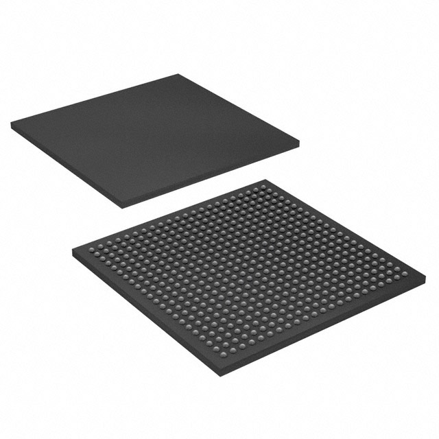
- I/O and Package — 327 I/O pins in a 484‑FBGA package (supplier package: 484‑UBGA, 19×19); surface-mount mounting for compact PCB integration.
- Low-Voltage Operation — Specified supply range of 1.15 V to 1.25 V to support low-power system designs.
- Commercial Temperature Grade — Rated for 0 °C to 85 °C operation for standard commercial applications.
- Clock Management — Family-level clocking resources include four phase-locked loops (PLLs) with multiple outputs and dynamic reconfiguration capability for flexible clock synthesis and distribution.
- Low-Power Family Architecture — Cyclone III family emphasizes low power through TSMC low-power process technology and silicon/software optimizations, helping to extend battery life and reduce system cooling requirements.
- System Reliability and Diagnostics — Family features include error-detection circuitry to monitor configuration memory integrity and detect single-event upsets (SEUs).
- Embedded Processing and IP — Supports the Cyclone III family’s ecosystem, including the Nios® II embedded processor and a broad collection of pre-built, verified IP cores.
- RoHS Compliant — Device is RoHS compliant.
Typical Applications
- High-volume, cost-sensitive consumer products — Use the device where low power and low cost are priorities while retaining significant programmable logic and memory resources.
- Portable and battery-powered systems — Low-voltage architecture and family-level low-power optimizations help extend battery life in handheld and portable designs.
- Embedded processing and custom peripherals — Integrate Nios® II soft processors and pre-built IP to implement application-specific control, protocol handling, or preprocessing functions.
- Interface and I/O-heavy systems — High I/O count and flexible I/O standards on the Cyclone III family make the device suitable for designs requiring extensive external interfacing.
Unique Advantages
- Significant logic capacity: 55,856 logic elements enable dense custom logic and feature integration on a single device, reducing BOM complexity.
- Substantial on-chip memory: Approximately 2.4 Mbits of embedded RAM supports buffering, packet processing, and local data storage without external memory.
- High I/O in a compact footprint: 327 I/Os in a 484‑FBGA (484‑UBGA, 19×19) package delivers broad connectivity while conserving PCB area.
- Low-voltage, power-aware operation: 1.15–1.25 V supply range and Cyclone III low-power design features help minimize system power consumption.
- Flexible clocking and reconfiguration: Multiple PLLs with dynamic reconfiguration provide robust clock management for diverse subsystems and interfaces.
- Established ecosystem: Access to Nios® II soft-core support and a wide selection of pre-verified IP cores accelerates development and reduces time-to-market.
Why Choose EP3C55U484C6?
The EP3C55U484C6 presents a balanced combination of programmable logic density, embedded memory, and I/O capability in a low-power Cyclone III architecture suitable for commercial, cost-sensitive designs. Its integration of clocking resources, on-chip memory, and a rich IP ecosystem makes it a practical choice for teams seeking to consolidate functionality, shorten BOMs, and accelerate development cycles.
Choose EP3C55U484C6 for projects that require substantial logic and memory resources, high I/O counts, and low-voltage operation within the commercial temperature range, backed by the Cyclone III device family features and platform support.
Request a quote or submit an inquiry to our sales team to check availability, lead times, and pricing for EP3C55U484C6. Provide your requirements and application details to receive tailored assistance and a formal quote.


Date Founded: 1968
Headquarters: Santa Clara, California, USA
Employees: 130,000+
Revenue: $54.23 Billion
Certifications and Memberships: ISO9001:2015, ISO14001:2015, ISO17025:2017, ISO27001:2022, ISO45001:2018, ISO50001:2018


